


DS_1209F_004
73S1209F Data Sheet
Rev. 1.2
55
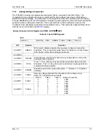
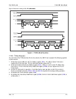
Figure 9 shows the timing of the I
2
C write mode.
C write mode.
1-7
8
9
10-17
18
ACK bit
ACK bit
STOP
condition
START
condition
1-7
8
9
10-17
18
ACK bit
ACK bit
STOP
condition
START
condition
SCL
SDA
LSB
MSB
LSB
MSB
Device Address
[7:0]
Write Data [7:0
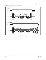
I2C_Interrupt
Start I2C
(CSR bit1)
Transfer length
(CSR bit0)
1-7
8
9
10-17
18
ACK bit
ACK bit
STOP
condition
START
condition
SCL
SDA
LSB
MSB
LSB
MSB
Device Address
[7:0]
Write Data [7:0]
I2C_Interrupt
Start I2C
(CSR bit1)
Transfer length
(CSR bit0)
Secondary Write
Data [7:0]
ACK bit
19-26
27
LSB
MSB
Figure 9: I
2
C Write Mode Operation
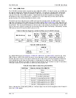
1.7.10.2 I
2
C Read Sequence
To read data on the I
2
C Master Bus from a slave device, the 80515 has to program the following registers
in this sequence:
1. Write slave device address to Device Address register (
). The data contains 7 bits device
address and 1 bit of op-code. The op-code bit should be written with a 1.
2. Write control data to Control and Status register (
). Write a 1 to bit 1 to start I
2
C Master Bus.
Also write a 1 to bit 0 if the Secondary Read Data register (
) is to be captured from the I
2
C
Slave device.
3. Wait for I
2
C interrupt to be asserted. It indicates that the read operation on the I
2
C bus is done.
Refer to information about the
and
registers for masking and flag operation.
4. Read data from the Read Data register (
5. Read data from Secondary Read Data register (
) if bit 0 of Control and Status register (
written with a 1.


