Page
5
of
11
TDK-Lambda
DBM20
INSTRUCTION MANUAL
PA640-04-01B
4-3.2 Ready and buffer signals as indicator of the
operation status of the buffer module. Ready signal will
change to logic high when the bulk electrolytic capacitors
charged up to more than 220Vdc typical after starts up,
and the green LED lights up. The RED LED will only
light up during buffering mode and at the same time the
buffer signal change to logic high. RED LED will be off
when the bulk electrolytic capacitors discharged to less
than 50Vdc typical.
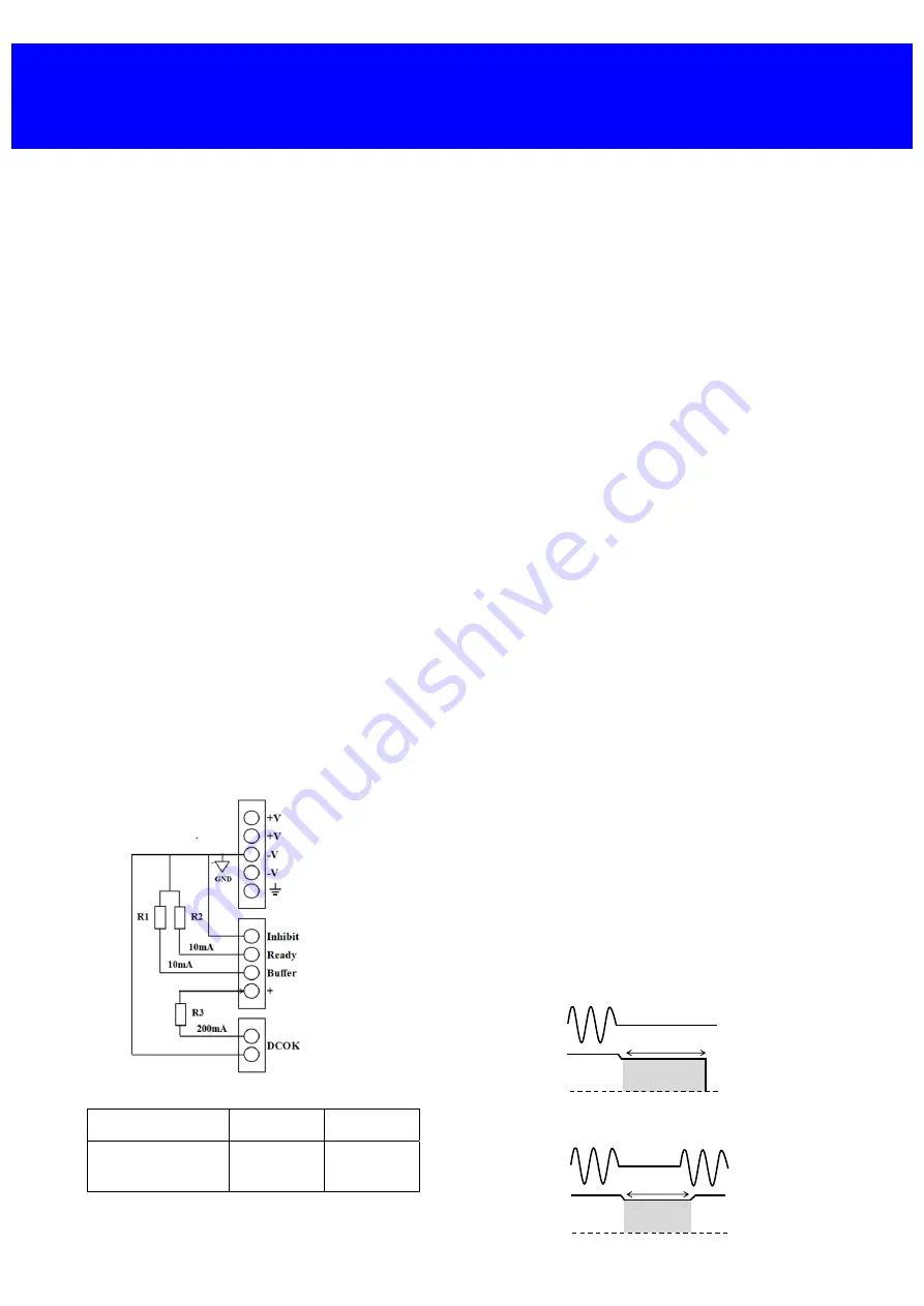
Ready and buffer signals with 10mA max. are common
supply type with voltage range 3.3 - 30V.
Caution on use :
a)
Kindly take note that both signals may be mistriggered
during brown out conditions.
b)
In Ready mode, buffer signal may appear if dynamic
load occurred.
4-3.3 Inhibit signal with 10mA max. is common
supply type with voltage range 3.3 - 30V.
Inhibit function can be activated by simply pulling the
inhibit signal line to logic low. The buffer unit will
immediate stop the existing charging/buffering
operation and start to discharge the energy stored in the
bulk electrolytic capacitors to the safe level in about 3 ~
5 seconds.
Caution on use :
Please do not touch the buffer module immediately after
the inhibit function because of high voltage might still
present across the bulk electrolytic capacitors.
Please refer to figure 6 for general connection diagram
for signals.
For example :
Common supply
R1 = R2
R3
12V±10%
1500Ω ±5%
(1W)
150Ω ±5%
(3W)
4-4. F
ixed Mode and Vin-1 Mode
Buffer module provides two option for buffer voltage
that is fixed mode and Vin-1 mode. Executed using
toggle switch to choose between the two options. (refer
to Figure 1).
At fixed mode the buffer voltage is set at 22.4V. While
in Vin-1 mode, the buffer voltage is typically 1V lower
than the regulated output voltage of the power supply
source. Vin-1 mode is suitable for adjustable output
upstream power supply, this is to keep buffer voltage as
close as possible to the regulated output voltage of the
power supply
4.5. Input Over Voltage Protection ( OVP )
Input OVP circuit will shut down the boost converter if
the input to the buffer module is greater than 30V. If the
input voltage drops back to the normal operating range
of 23 - 30V, the buffer module will operate as per normal
again.
4-6. Over Current Protection ( OCP )
The OCP function is provided for the buffer voltage. When
the buffering current exceeds 105% of the maximum DC
buffer current specification, OCP operation will be
activated. The buffering current will be automatically
recovered when overload condition is removed.
4-7.
Parallel Operation
The buffer module can be connected in parallel to increase
the buffer time. Please refer to wiring diagram shown in
3-1 (2) for parallel connection. The total output current
and charge current must not exceed the maximum output
current of the upstream power supply. The voltage may
drop due to the overcurrent protection of the upstream
power supply.
4-8. Series
Operation
Not possible.
4-9. Buffer
Module Operation
The product can be used to :
a)
To extend the hold up time after AC loss.
Buffer Module
AC
DC
GND
buffer time
b)
To bridge the mains failure
Buffer Module
AC
DC
GND
buffer time
Figure 6


