background image

2-34


X7SB3/X7SB3-F User's Manual

J27

J8

JLAN1

B1

COM2

JWOR

JAR

JPF

J3P

J45

J44

JPG1

JPL1

JPUSB1

JPS2

JPS1

JLED1

JWD

JPW1

JWOL

3-SGPIO2

Fan5

Fan1

Fan4

Fan2

JBT1

PW4

PCI1

SAS7

SAS0

SAS5

SAS6

SAS4

SAS3

SAS2

SAS1

SPKR1

J48

J47

JD1

LE2

LE4

LE5

LE1

COM1

JF1

JPW2

DIMM4

DIMM3

DIMM2

DIMM1

CPU

KB/MOUSE

VGA

LE3

USB2

USB6/7

USB4/5             

JLAN2

Battery

LAN

CTRL1

PCI-E x8

LAN

CTRL2

Winbond

IPMI/VGA CTRL

Winbond
83627DHG

SI/O

JI2C2

JI2C1

Intel
ICH9

(South Bridge)

3-SGPIO1

LSI

1068E

SAS CTRL

USB3

Floppy

FP

 CTRL

Fan3

Intel

3210 MCH

(North Bridge)

JS1

JS2

I-SA

TA0

I-SA

TA1

PCI 33 MHz

BIOS

82574L

Intel

82574L

Intel

WPCM450-R

X7SB3

24-pin ATX PWR

8-pin PWR

I-Button

JPL2

JPB

JL1

LED1

DIMM1A

DIMM2A

DIMM1B

DIMM2B

USB0/1

IPMI LAN  (X7SB3-F)

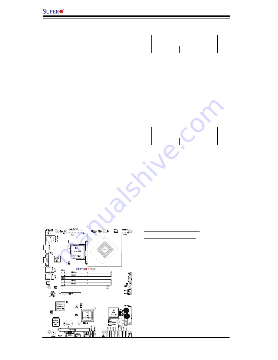
A. LE5:  SAS Heartbeat LED
B. LED1: SAS Activity LED

A

B

SAS Heartbeat LED 

A SAS Heartbeat LED is located at LE5. 
When  LE5  blinks,  SAS  connectors  are 
ready for use. Refer to the table on the 
right for details. Also see the layout below 
for the LED location. 

SAS Heartbeat LED Indicator (LE5)

LED Settings

Blinking: Yellow

SAS is ready for use

SAS Activity LED 

A SAS Activity LED is located at LED1. 
When LED1 blinks, SAS is active. Refer 
to the table on the right for details. Also 
see  the  layout  below  for  the  LED  loca-
tion. 

SAS Activity LED Indicator (LED1)

LED Settings

Blinking: Green

SAS is active

Содержание X7SB3

Страница 1: ...SUPER X7SB3 USER S MANUAL Revision 1 0b X7SB3 F...

Страница 2: ...UPER MICRO COMPUTER INC SHALL NOT HAVE LIABILITY FOR ANY HARDWARE SOFTWARE OR DATA STORED OR USED WITH THE PRODUCT INCLUDING THE COSTS OF REPAIRING REPLACING INTEGRATING INSTALLING OR RECOVERING SUCH...

Страница 3: ...herboard for the most recent updates This product is intended to be professionally installed and serviced by a technician Manual Organization Chapter 1 introduces the motherboard providing information...

Страница 4: ...eral Information support supermicro com Technical Support Web Site www supermicro com Europe Address Super Micro Computer B V Het Sterrenbeeld 28 5215 ML s Hertogenbosch The Netherlands Tel 31 0 73 64...

Страница 5: ...Contacting Supermicro v Notes...

Страница 6: ...pply 1 12 1 7 Super I O 1 13 1 8 Overview of the Winbond WPCM450 Controller 1 13 Chapter 2 Installation 2 1 Static Sensitive Devices 2 1 Precautions 2 1 Unpacking 2 1 2 2 Mounting the Motherboard in t...

Страница 7: ...O Connections 2 18 ATX PS 2 Keyboard and PS 2 Mouse Ports 2 18 Serial Ports 2 18 Universal Serial Bus USB 2 19 GLAN 1 2 Ethernet Ports and IPMI dedicated LAN Port 2 19 VGA Connector 2 20 Serial ATA P...

Страница 8: ...es 3 1 Before Power On 3 1 No Power 3 1 No Video 3 2 Losing the System s Setup Configuration 3 2 3 2 Technical Support Procedures 3 2 3 3 Frequently Asked Questions 3 3 3 4 Returning Merchandise for S...

Страница 9: ...ith the highest standards in quality and performance Check that the following items have all been included with your motherboard If anything listed here is damaged or missing contact your retailer All...

Страница 10: ...Image Note The drawings and pictures shown in this manual were based on the latest PCB Revision available at the time of publishing of the manual The motherboard you ve received may or may not look e...

Страница 11: ...JPL1 JPUSB1 JPS2 JPS1 JLED1 JWD JPW1 JWOL 3 SGPIO2 Fan5 Fan1 Fan4 Fan2 JBT1 PW4 PCI1 SAS7 SAS0 SAS5 SAS6 SAS4 SAS3 SAS2 SAS1 SPKR1 J48 J47 JD1 LE2 LE4 LE5 LE1 COM1 JF1 JPW2 DIMM4 DIMM3 DIMM2 DIMM1 CPU...

Страница 12: ...el 82574L Intel WPCM450 R X7SB3 24 pin ATX PWR 8 pin PWR I Button JPL2 JPB JL1 LED1 DIMM1A DIMM2A DIMM1B DIMM2B USB0 1 IPMI LAN X7SB3 F X7SB3 X7SB3 F Quick Reference Jumper Label Description Default S...

Страница 13: ...8 12V 8 Pin Auxiliary PWR Connector JWOL 26 Wake On LAN Header JWOR 16 Wake On Ring Header KB MS 1 PS 2 Keyboard Mouse PW4 X7SB3 F 62 Power Supply SMB I2 C Connector SAS 0 7 35 42 Serial_Attached SCSI...

Страница 14: ...OS 16 Mb Phoenix SPI Flash EEPROM DMI 2 3 PCI 2 2 APM 1 2 ACPI 1 0 2 0 3 0 Plug and Play PnP USB Key board support and SMBIOS 2 3 PC Health Monitoring Onboard voltage monitors for CPU cores Memory Chi...

Страница 15: ...only One floppy port interface supports 1 44 MB Two COM ports 1 header 1 port supports Fast UART 16550 connection Up to eight USB 2 0 Universal Serial Bus two backpanel connectors two front panel int...

Страница 16: ...PCM450R ADDR CTRL CTRL ADDR DATA DATA LPC DDR2_800 667 DMI DIMM_CHA CHB S ATA 300 2 SATA PORTS CK505 CLK MCH PCIE_x8 FSB 1333 1066 800MHz LPC LSI SAS 1068E 8 X SAS PORTS PCIE_x1 GLAN1 82574L PCIE_x1 V...

Страница 17: ...SDRAM Intel ICH9 System Features The I O Controller ICH9 provides the data buffering and interface arbitration re quired for the system to operate efficiently It also provides the bandwidth needed for...

Страница 18: ...Standby and VBAT voltages continuously Once a voltage becomes unstable a warning is given or an error message is sent to the screen Users can adjust the voltage thresholds to define the sensitivity of...

Страница 19: ...ecifi cation defines a flexible and abstract hardware interface that provides a standard way to integrate power management features throughout a PC system including its hardware operating system and a...

Страница 20: ...motherboard has a 3 pin header WOL to connect to the 3 pin header on a Network Interface Card NIC that has WOL capability In addition an onboard LAN controller can also support WOL without any connec...

Страница 21: ...legacy and ACPI power manage ment through an SMI or SCI function pin It also features auto power management to reduce power consumption 1 8 Overview of the Winbond WPCM450 Controller The Winbond WPCM4...

Страница 22: ...1 14 X7SB3 X7SB3 F User s Manual Notes...

Страница 23: ...o not touch its components peripheral chips memory modules or gold contacts When handling chips or modules avoid touching their pins Put the motherboard and peripherals back into their antistatic bags...

Страница 24: ...nting holes on the motherboard Refer to the layout below for the locations of the mounting holes The holes marked with arrows are the mounting holes on this motherboard Pan head 6 32 x 5 mm 0 197 Loca...

Страница 25: ...ds have standard mounting holes to fit different types of chassis Make sure that the locations of all the mounting holes for both motherboard and chassis match 2 Some components are very close to the...

Страница 26: ...Notes Always connect the power cord last and always remove it before adding 1 removing or changing any components Make sure that you install the pro cessor into the CPU socket before you install the...

Страница 27: ...side of the triangle cutout on the socket Once aligned carefully lower the 3 CPU straight down to the socket Do not drop the CPU on the socket Do not move the CPU horizontally or vertically Do not ru...

Страница 28: ...on the retention mechanism Screw in two diagonal screws ie the 1 3 and the 2 screws until just snug do not fully tighten the screws to avoid possible damage to the CPU Finish the installation by full...

Страница 29: ...ght and gently wriggle the heatsink to loosen it from the CPU Do not use excessive force when wriggling the heatsink Once the heatsink is loosened remove 3 the heatsink from the CPU socket Clean the s...

Страница 30: ...te for other information Memory Support The X7SB3 X7SB3 F supports up to 8 GB Unbuffered ECC Non ECC DDR2 800 667 MHz in 4 DIMMs Populating memory slots of the same bank with a pair or pairs of memory...

Страница 31: ...ical Memory Remaining Available 4 GB Total System Memory Firmware Hub flash memory System BIOS 1 MB 3 99 Local APIC 4 KB 3 99 Area Reserved for the chipset 2 MB 3 99 I O APIC 4 Kbytes 4 KB 3 99 PCI En...

Страница 32: ...e the graphics below for the colors and locations of the various I O ports Back Panel Connectors IO Ports Back Panel I O Port Locations and Definitions 1 2 3 4 5 6 7 8 9 Back Panel Connectors 1 Keyboa...

Страница 33: ...pecifically for use with Supermicro server chassis See the figure below for the descriptions of the various control panel buttons and LED indicators Refer to the following section for descriptions and...

Страница 34: ...onnection is located on pins 15 and 16 of JF1 Refer to the table on the right for pin definitions NMI Button The non maskable interrupt button header is located on pins 19 and 20 of JF1 Refer to the t...

Страница 35: ...s HDD LED The HDD LED connection is located on pin 14 of JF1 Attach a hard drive LED cable here to display disk activ ity See the table on the right for pin definitions HDD UID LED Pin Definitions JF1...

Страница 36: ...vanced warnings of chassis overheating or fan failure Refer to the table on the right for pin definitions Power Fail LED The Power Fail LED connection is located on pins 5 and 6 of JF1 Refer to the ta...

Страница 37: ...to function as a suspend button with a setting in the BIOS see Chapter 4 To turn off the power when set to suspend mode press the button for at least 4 seconds Refer to the table on the right for pin...

Страница 38: ...8 pin Processor PWR A B 2 6 Connecting to the Headers and Connectors Power Connectors ATX Power Connector A 24 pin main power supply connector JPW1 and an 8 pin CPU PWR connector JPW2 are located on...

Страница 39: ...A1 PCI 33 MHz BIOS 82574L Intel 82574L Intel WPCM450 R X7SB3 24 pin ATX PWR 8 pin PWR I Button JPL2 JPB JL1 LED1 DIMM1A DIMM2A DIMM1B DIMM2B USB0 1 IPMI LAN X7SB3 F Fan Headers The X7SB3 X7SB3 F has f...

Страница 40: ...IMM2A DIMM1B DIMM2B USB0 1 IPMI LAN X7SB3 F I O Connections ATX PS 2 Keyboard and PS 2 Mouse Ports The ATX PS 2 keyboard and the PS 2 mouse are located on the I O back plane See the table on the right...

Страница 41: ...essible USB connections USB 2 and USB 3 are Type A connectors USB 4 5 and USB 6 7 are Front Panel Internal Ports See the tables on the right for pin definitions Note To comply with FCC requirements pl...

Страница 42: ...pin ATX PWR 8 pin PWR I Button JPL2 JPB JL1 LED1 DIMM1A DIMM2A DIMM1B DIMM2B USB0 1 IPMI LAN X7SB3 F SATA Port Pin Definitions Pin Definition Pin Definition 1 Ground 2 TX 3 TX 4 Ground 5 RX 6 RX 7 Gro...

Страница 43: ...R JPF J3P J45 J44 JPG1 JPL1 JPUSB1 JPS2 JPS1 JLED1 JWD JPW1 JWOL 3 SGPIO2 Fan5 Fan1 Fan4 Fan2 JBT1 PW4 PCI1 SAS7 SAS0 SAS5 SAS6 SAS4 SAS3 SAS2 SAS1 SPKR1 J48 J47 JD1 LE2 LE4 LE5 LE1 COM1 JF1 JPW2 DIMM...

Страница 44: ...3210 MCH North Bridge JS1 JS2 I SATA0 I SATA1 PCI 33 MHz BIOS 82574L Intel 82574L Intel WPCM450 R X7SB3 24 pin ATX PWR 8 pin PWR I Button JPL2 JPB JL1 LED1 DIMM1A DIMM2A DIMM1B DIMM2B USB0 1 IPMI LAN...

Страница 45: ...WPCM450 R X7SB3 24 pin ATX PWR 8 pin PWR I Button JPL2 JPB JL1 LED1 DIMM1A DIMM2A DIMM1B DIMM2B USB0 1 IPMI LAN X7SB3 F Wake On Ring The Wake On Ring header is located at JWOR This header is used to w...

Страница 46: ...Intel WPCM450 R X7SB3 24 pin ATX PWR 8 pin PWR I Button JPL2 JPB JL1 LED1 DIMM1A DIMM2A DIMM1B DIMM2B USB0 1 IPMI LAN X7SB3 F Speaker A Speaker header is located at JD1 Con nect a cable to pins 1 4 of...

Страница 47: ...CI 33 MHz BIOS 82574L Intel 82574L Intel WPCM450 R X7SB3 24 pin ATX PWR 8 pin PWR I Button JPL2 JPB JL1 LED1 DIMM1A DIMM2A DIMM1B DIMM2B USB0 1 IPMI LAN X7SB3 F A A PWR SMB B I Button Power I2 C Conne...

Страница 48: ...068E SAS CTRL USB3 Floppy FP CTRL Fan3 Intel 3210 MCH North Bridge JS1 JS2 I SATA0 I SATA1 PCI 33 MHz BIOS 82574L Intel 82574L Intel WPCM450 R X7SB3 24 pin ATX PWR 8 pin PWR I Button JPL2 JPB JL1 LED1...

Страница 49: ...JPS1 JLED1 JWD JPW1 JWOL 3 SGPIO2 Fan5 Fan1 Fan4 Fan2 JBT1 PW4 PCI1 SAS7 SAS0 SAS5 SAS6 SAS4 SAS3 SAS2 SAS1 SPKR1 J48 J47 JD1 LE2 LE4 LE5 LE1 COM1 JF1 JPW2 DIMM4 DIMM3 DIMM2 DIMM1 CPU KB MOUSE VGA LE3...

Страница 50: ...B JL1 LED1 DIMM1A DIMM2A DIMM1B DIMM2B USB0 1 IPMI LAN X7SB3 F 2 7 Jumper Settings Explanation of Jumpers To modify the operation of the mother board jumpers can be used to choose between optional set...

Страница 51: ...h Dog Enable Watch Dog Enable Disable Watch Dog JWD is a system monitor that reboots the system when a software appli cation hangs Close pins 1 2 to reset the system if an application hangs Close pins...

Страница 52: ...South Bridge 3 SGPIO1 LSI 1068E SAS CTRL USB3 Floppy FP CTRL Fan3 Intel 3210 MCH North Bridge JS1 JS2 I SATA0 I SATA1 PCI 33 MHz BIOS 82574L Intel 82574L Intel WPCM450 R X7SB3 24 pin ATX PWR 8 pin PW...

Страница 53: ...SAS5 SAS6 SAS4 SAS3 SAS2 SAS1 SPKR1 J48 J47 JD1 LE2 LE4 LE5 LE1 COM1 JF1 JPW2 DIMM4 DIMM3 DIMM2 DIMM1 CPU KB MOUSE VGA LE3 USB2 USB6 7 USB4 5 JLAN2 Battery LAN CTRL1 PCI E x8 LAN CTRL2 Winbond IPMI VG...

Страница 54: ...L Intel 82574L Intel WPCM450 R X7SB3 24 pin ATX PWR 8 pin PWR I Button JPL2 JPB JL1 LED1 DIMM1A DIMM2A DIMM1B DIMM2B USB0 1 IPMI LAN X7SB3 F A SAS Enable B SAS RAID Mode Select A B SAS Enable Disable...

Страница 55: ...bit Ethernet LAN port has two LEDs The yellow LED indicates activity while the Link LED may be green amber or off to indicate the speed of the connection See the tables on the right for more informati...

Страница 56: ...A1 PCI 33 MHz BIOS 82574L Intel 82574L Intel WPCM450 R X7SB3 24 pin ATX PWR 8 pin PWR I Button JPL2 JPB JL1 LED1 DIMM1A DIMM2A DIMM1B DIMM2B USB0 1 IPMI LAN X7SB3 F A LE5 SAS Heartbeat LED B LED1 SAS...

Страница 57: ...outh Bridge 3 SGPIO1 LSI 1068E SAS CTRL USB3 Floppy FP CTRL Fan3 Intel 3210 MCH North Bridge JS1 JS2 I SATA0 I SATA1 PCI 33 MHz BIOS 82574L Intel 82574L Intel WPCM450 R X7SB3 24 pin ATX PWR 8 pin PWR...

Страница 58: ...loppy and hard disk drive cables The floppy disk drive cable has seven twisted wires A red mark on a wire typically designates the location of pin 1 A single floppy disk drive ribbon cable has 34 wire...

Страница 59: ...s Disconnect all ribbon wire cables from the motherboard including those for 2 the keyboard and mouse Remove all add on cards Install a CPU in CPU Socket and connect the chassis speaker and the power...

Страница 60: ...DIMMs of different speeds or types have been installed Also make sure that the BIOS setup is configured for the fastest speed of RAM used It is recommended to use the same RAM speed for all DIMMs in...

Страница 61: ...utors For immediate assistance please have your account number ready when placing a call to our technical support department We can be reached by e mail at support supermicro com or by fax at 408 503...

Страница 62: ...nt possible system boot failure When the BIOS flashing screen is completed the system will reboot and will show Press F1 or F2 At this point you will need to load the BIOS defaults Press F1 to go to t...

Страница 63: ...the manufacturer the RMA number should be prominently displayed on the outside of the shipping carton and mailed prepaid or hand carried Shipping and handling charges will be applied for all orders t...

Страница 64: ...3 6 X7SB3 X7SB3 F User s Manual Notes...

Страница 65: ...The CMOS memory requires very little electrical power When the computer is turned off a backup battery provides power to the CMOS logic enabling it to retain system parameters Each time when the comp...

Страница 66: ...n or 1 When the message shown below appears briefly at the bottom of the screen 2 during the POST Power On Self Test press the Delete key to activate the main Setup menu Press the Delete key to enter...

Страница 67: ...number of the BIOS Legacy Diskette A This setting allows the user to set the type of floppy disk drive installed as diskette A The options are Disabled 360Kb 5 25 in 1 2MB 5 25 in 720Kb 3 5 in 1 44 1...

Страница 68: ...Set the correct configurations accordingly The items included in the sub menu are Type This feature allows the user to select the type of a drive specified Select Auto to allow the BIOS to automatical...

Страница 69: ...are installed 32 Bit I O Select Enable to enable the function of 32 bit IDE data transfer The options are Enabled and Disabled Note The default setting changes when different devices are installed Tra...

Страница 70: ...Enable and Disabled Quiet Boot This setting allows you to Enable or Disable the graphic logo screen display at bootup QuickBoot Mode If enabled this feature will speed up the POST Power On Self Test r...

Страница 71: ...ure is set enabled you will also need to enable the JPUSB1 jumper by closing pins 1 2 Please refer to Page 1 4 and Chapter 2 for more details The default setting is Disabled Power Loss Control This se...

Страница 72: ...mance The options are Disabled and Enabled Core Multi Processing Available when supported by the CPU Set to Enabled to use a processor s Second Core and beyond Please refer to Intel s web site for mor...

Страница 73: ...systems in one physical computer The options are Enabled and Disabled Note If there is any change to this setting you will need to power off and restart the system for the change to take effect Please...

Страница 74: ...he Intel platforms providing the user with greater reliability security and availability in networking and data sharing The settings are Enabled and Disabled High Precision Event Time Select Yes to ac...

Страница 75: ...nto a buffer a storage area in the Static DROM SDROM or to be written into L1 L2 cache inside the CPU to speed up CPU operations Select Uncached to disable this function Select Write Through to al low...

Страница 76: ...uration Access the submenu to make changes to the following settings for PCI devices PCI 32 Slot PCI Express x8 Slot Access the submenu for each of the settings above to make changes to the following...

Страница 77: ...r the installation of a new software you might want to change this setting and try again A different OS requires a different Bus Master clock rate I O Device Configuration Access the submenu to make c...

Страница 78: ...is setting allows you to select the base I O address for Serial Port B The options are 3F8 2F8 3E8 and 2E8 Interrupt This setting allows you to select the IRQ interrupt request for Serial Port B The o...

Страница 79: ...I Event Logs Select Yes and press Enter to clear all DMI event logs The options are Yes and No Console Redirection Access the submenu to make changes to the following settings COM Port Address This it...

Страница 80: ...sole Connection This item allows you to decide how console redirection is to be connected either Direct or Via Modem Continue CR after POST Select on to continue with console redirection after the POS...

Страница 81: ...shold temperature as predefined by the CPU manufacturer to give the CPU and system fans additional time needed for CPU and system cooling CPU Temperature The CPU Temperature feature will display the C...

Страница 82: ...embedded by unique temperature information that the motherboard can read This Temperature Threshold or Temperature Tolerance has been assigned at the factory and is the baseline on which the motherboa...

Страница 83: ...n Server and 5 4 pin Workstation Voltage Monitoring The following items will be monitored and displayed VcoreA 12V 12V V_DIMM 5V 3 3V 3 3Vsb and Vbatt Note In the Windows OS environment the Supero Doc...

Страница 84: ...The options are Enabled and Disabled Clear System Event Logging Enable this function to force the BIOS to clear the system event logs during the next cold boot The options are Enabled and Disabled Exi...

Страница 85: ...hen OS Boot Watch Dog is set to Disabled Time Out Option This item allows the user to decide what action to take in an event of a system boot failure The options are No Action Reset Power Off and Powe...

Страница 86: ...4 22 X7SB3 X7SB3 F User s Manual Realtime Sensor Data X7SB3 F only This feature display information from motherboard sensors such as tempera tures fan speeds and voltages of various components...

Страница 87: ...gging is disabled this item will be ignored by the firmware IP Address Source This item allows the user to select the IP address source for the connection The options are DHCP and Static This item dis...

Страница 88: ...supervisor password has been entered for the system User Password Is This item indicates if a user password has been entered for the system Clear means such a password has not been used and Set means...

Страница 89: ...nable Write Protect the boot sector on the hard drives to protect against viruses Password on Boot This setting allows you to require a password to be entered when the system boots up The options are...

Страница 90: ...tions for the devices included in the candidate list above are currently disabled Use a key or a key to move the device up or down Use the f key or the r key to specify the type of an USB device eithe...

Страница 91: ...Discarding Changes Highlight this item and hit Enter to exit the BIOS Setup utility without saving any changes you may have made Load Setup Defaults Highlight this item and hit Enter to load the defau...

Страница 92: ...4 28 X7SB3 X7SB3 F User s Manual Notes...

Страница 93: ...BIOS Recoverable POST Errors When a recoverable type of error occurs during POST the BIOS will display a POST code that describes the problem BIOS may also issue one of the following beep codes 1 long...

Страница 94: ...A 2 X7SB3 X7SB3 F User s Manual Notes...

Страница 95: ...ows XP 2000 2003 OS Insert Microsoft s Windows XP 2000 2003 Setup CD in the CD Driver and the 1 system will start booting up from CD Continue with the OS installation The Windows OS Setup screen will...

Страница 96: ...B 2 X7SB3 X7SB3 F User s Manual Notes...

Страница 97: ...and drivers that have not yet been installed To install these software programs and drivers click the icons to the right of these items Driver Tool Installation Display Screen Note Click the icons sh...

Страница 98: ...tem voltages and fan status See the Figure below for a display of the Supero Doctor III interface Note 1 Both default username and password are ADMIN Note 2 In the Windows OS environment the Supero Do...

Страница 99: ...n II Remote Control Note SD III Software can be downloaded from our Web site at ftp ftp supermicro com utility Supero_Doctor_III You can also download SDIII User s Guide at http www supermicro com PRO...

Страница 100: ...C 4 X7SB3 X7SB3 F User s Manual Notes...

Страница 101: ...expected to result in significant injury or loss of life or catastrophic property damage Accordingly Supermicro disclaims any and all liability and should buyer use or sell such products for use in su...

Отзывы: