


2-18
PDSMi
User's
Manual
PCI 32 Bit/33 MHz
S
UPER PDSMi
REV 1.0
®
Pentium Dual
Core CPU
LGA 775
KB/MS
COM1
GLAN1
E7230
(North Bridge)
LAN
CTRL
J P L 1
Fan4
Buzzer
JLED
24-Pin ATX PWR
ICH7R
JF1
(South Bridge)
J31
J28
Fan6/CPU Fan
8-pin PWR
Battery
J 9
FP CTRL
USB 1/2
J15
VGA
JG1
GLAN2
LAN
CTRL
S I/O
COM2
J P L 2
Printer
Floppy
Slot1
SXB -E1 PCI-Ex8
DIMM 2B
PCI-X 133 MHz
BIOS
PXH-V
IPMI
Mukilteo
JPW1
J 3 0
J 2 7
IDE
J 4
J 3
IDE (Primary)
JWOR
LE1
JBT1
USB3/4 USB5/6
JWF1
JPG1
JPF
J W D
WOL
Fan3
Fan2
DIMM 1B
DIMM 2A
DIMM 1A
DIMM 1
DIMM 2
DIMM 3
DIMM 4
Fan1
JPW2
VGA
CTRL
Slot6
L E 3
L E 4
SATA0
SATA1
SATA2
SATA3
(*Compact Flash Card only)
J L 1
JP3
J I
2
C 1
J I
2
C 2
Fan5
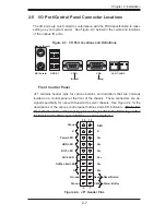
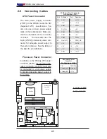
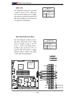
Power LED
The Power LED connector is desig-
nated JLED. This connection is used
to provide LED Indication of power
being supplied to the system. See the
table on the right for pin defi nitions.
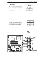
VGA Connector
A VGA connector (JG1) is located next
to the COM1 port on the IO backplane.
Refer to the board layout below for
the location.
PWR LED
Pin Defi nitions
Pin# Defi nition
1
+5V
2
Key
3
Ground
A
B
A. VGA
B. PWR LED
Содержание PDSMi
Страница 1: ...PDSMi USER S MANUAL Revision 1 0a ...
Страница 70: ...4 22 PDSMi User s Manual Notes ...
Страница 82: ...B 6 PDSMi User s Manual Notes ...
Страница 100: ...C 18 PDSMi User s Manual Notes ...


