1-34
IC
VGN-
S36C/S36GP/S36LP/S36SP/S36TP/S38CP/
S52B/
S62PS/S62PSY/S62S/
S350F/S350FP/
S360/S360P/
S370F
(J/AM
/AO
)
Confidential
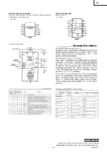
RG82855PMSL752 (INTEL)
IntelR 855PM CHIPSET MEMORYCONTROLLER HUB (MCH) DDR 200/
266MHz
– TOP VIEW –
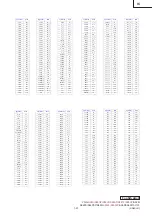
29
28
27
26
25
24
23
22
21
20
19
18
17
16
15
14
13
12
11
10
9
8
7
6
5
4
3
2
1
AJ
VSS
VCC1_5
VCCP
VCCP
VCCP
VSS
VSS
VSS
VSS
VSS
VSS
VSS
VSS
AJ
AH
SBA0
SBA1
G_GNT
#
VSS
VSS
VSS
HD61#
HD57#
HD49#
HD44#
DBI2#
HD24#
HD31#
HD29# HD20#
AH
AG
VCC1_5 SBA2
SBA3
ST2
ST0
G_REQ
#
VCCP
VSS
VCCP
VSS
VCCP
VSS
HD56# HD55# HD54# HD52# HD48# HD45# HD42# HD43# HD38# HD27# HD28#
HDSTB
P1#
DBI1#
HD16# HD22# HD17#
VSS
AG
AF
SBSTB SBSTB#
VSS
ST1
VCC1_5 PIPE#
VSS
VCCP
VSS
VCCP
VSS
HD59#
VSS
HD51#
VSS
HD47#
VSS
HD41#
VSS
HD30#
VSS
HDSTB
N1#
VSS
HD14# HD11#
AF
AE
VSS
SBA4
SBA5 VCC1_5 SBA7
SBA6
WBF#
RBF#
VCCP
VSS
VCCP
VSS
CPURS
T#
HD63# HD60# HD53# HD46# HD40#
HDSTB
P2#
HD36# HD34# HD19# HD18# HD25# HD10#
VSS
HD8#
HD15#
VSS
AE
AD
NC
NC
GRCOM
P
G_AD31 VCC1_5
VSS
VCC1_5 VCCP
VSS
VCCP
HD62#
VSS
DBI3#
VSS
HSWN
G1
VSS
HDSTB
N2#
VSS
HD37#
VSS
HD23#
VSS
DBI0#
HDSTB
N0#
HDSTB
P0#
AD
AC
VCC1_5
AD_ST
B1#
AD_ST
B1
VSS
G_AD28 G_AD29
VSS
G_AD30
VSS
VSS
VCCP
VSS
HD58#
HDSTB
P3#
HDSTB
N3#
HD50#
HRCOM
P1
HD33# HD32# HD35# HD39# HD26# HD21# HD12#
HD5#
VSS
HD13#
HRCOM
P0
VSS
AC
AB
G_AD20 G_AD22 G_AD19 G_AD27 G_AD24
VSS
VCC1_5 VCCP
VSS
VCCP
VSS
HVREF
VSS
VCCP
VSS
HVREF
VSS
VCCP
VSS
VCCP
HD9#
VSS
HD1#
HD4#
HD3#
AB
AA
VSS
G_AD18 G_AD21 VCC1_5 G_AD26 G_AD25
G_CBE
3#
VCC1_5
AGPRE
F
HVREF
VSS
HSWN
G0
HD7#
HD2#
VSS
HD6#
HD0#
VSS
AA
Y
G_AD16 G_AD17
G_CBE
2#
G_FRA
ME#
G_AD23
VSS
DPWR# BPRI#
VSS
HIT#
DEFER
#
HITM#
Y
W
VCC1_5
G_DEV
SEL#
G_IRDY
#
VSS
G_PAR
G_TRD
Y#
G_STO
P#
VCC1_5
VSS
RS0#
RS2#
RS1#
VSS
HLOCK
#
DRDY#
VSS
W
V
G_AD9 G_AD8
G_CBE
0#
G_AD15
G_CBE
1#
VSS
DPSLP
#
BR0#
VSS
DBSY#
HTRDY
#
BNR#
V
U
VSS
G_AD7 G_AD6 VCC1_5 G_AD14 G_AD13 G_AD11 VCC1_5
VSS
VCC
VSS
VCC
VSS
VSS
ADS#
HA3#
HREQ3
#
VSS
HA6#
HREQ0
#
VSS
U
T
G_AD5 G_AD4 G_AD2 G_AD12 G_AD10
VSS
VCCGA
VSS
VCC
VSS
VCCHA
VCCP
HREQ1
#
VSS
HA4#
HREQ4
#
HA9#
T
R
VCC1_5 G_AD1 G_AD0
VSS
G_AD3
AD_ST
B0
AD_ST
B0#
VCC1_5
VSS
VCC
VSS
VCC
VSS
VSS
HREQ2
#
HA13#
HADST
B0#
VSS
HA7#
HA5#
VSS
R
P
HLRCO
MP
HI_REF
HI_0
HI_1
HI_3
66IN
VCC
VSS
VCC
VSS
VCC
HVREF HA8#
VSS
HA12# HA10# HA11#
P
N
VSS
HI_9
HI_2
VCC1_8 HI_STB
HI_STB
#
VCC1_8
VSS
VSS
VCC
VSS
VCC
VSS
VSS
HADST
B1#
HA24# HA15#
VSS
HA16# HA14#
VSS
N
M
HI_8
HI_4
HI_5
HI_10
VSS
VCC1_8
VCCP HVREF
VSS
HA20# HA19# HA18#
M
L
VCC1_8
HI_6
HI_7
VSS
VCC1_8
VSS
VCCSM
VSS
VSS
HA29# HA25# HA21#
VSS
HA28# HA26#
VSS
L
K
VSS
VCCSM SCK#0 VCCSM SCK5 VCCSM
BLCK# VCCSM
VSS
HA27# HA30# HA22#
K
J
VSS
SMRCO
MP
RSTIN#
VSS
SCK0
SCK#3 SCK#5
VSS
SMVRE
F
SMVRE
F
BLCK
VSS
VCCSM HA31#
VSS
HA17# HA23#
VSS
J
H
RSVD
TESTIN
#
SDQ4 VCCSM SCKE2 VCCSM
VSS
VCCSM
VSS
VCCSM
VSS
VCCSM
VSS
VCCSM
VSS
VCCSM
VSS
VCCSM
VSS
VCCSM RSVD
VSS
VCCSM ETS#
RSVD
H
G
VCCSM SDQ0
SDQ5
VSS
SCK3
SCK2 SCKE0 RSVD SMA12 SMA7
SMA8
SMA4
SMA3
RSVD
RCVENI
N#
RCVEN
OUT#
SBS1
SBS0
SWE#
RSVD
RSVD SCAS# SCK#4
SCK4
SCK1
SDQ63 RSVD
RSVD VCCSM
G
F
SDQ1 SDQS0 SDQ6
VSS
SCKE3 VCCSM SMA9
VSS
SMA6 VCCSM SMA1 VCCSM
VSS
VCCSM SMA10
VSS
SRAS# VCCSM SCS#2
VSS
SCS#1
VSS
SCK#1 SDQ58 SDQ59
F
E
VSS
SDQ3
SDQ8
VSS
SDQ15 SCK#2 SDQ17 SCKE1 SDQ19 SMA11 SDQ29 SMA5 SDQ31 SMA2 SDQS8
VSS
SDQ32 SMA0 SDQ44 SDQ40 SCS#0 SDQ43 SCS#3 SDQ52 VCCSM SDQ55 SDQS7 SDQ62
VSS
E
D
SDQ13 SDQ14 VCCSM SDQ16 VCCSM SDQ22
VSS
SDQ25 VCCSM SDQ27
VSS
SDQ65 VCCSM SDQ71
VSS
SDQS4 VCCSM SDQ39
VSS
SDQ42 VCCSM SDQ49
VSS
SDQ50 SDQ57
D
C
VCCSM SDQ2
SDQ9 SDQS1 SDQ11 SDQ20 SDQS2 SDQ18 SDQ24 SDQ28 SDQ26 SDQ30 SDQ69 SDQ64 SDQ70 SDQ67 SDQ37 SDQ33 SDQ38 SDQ35 SDQ41 SDQS5 SDQ47 SDQ48 SDQS6 SDQ54 SDQ56 SDQ61 VCCSM
C
B
SDQ7 SDQ12
SDQ10
SDQ21
SDQ23
SDQS3
SDQ68
SDQ66
SDQ36
SDQ34
SDQ45
SDQ46
SDQ53
SDQ51 SDQ60
B
A
VSS
VCCSM
VSS
VCCSM
VSS
VCCSM
VSS
VCCSM
VSS
VCCSM
VSS
VCCSM
VSS
A
29
28
27
26
25
24
23
22
21
20
19
18
17
16
15
14
13
12
11
10
9
8
7
6
5
4
3
2
1
2.1. Host
Interface
Signals
Note:
Unless otherwise noted, the voltage level for all signals in this interface is tied to the termination voltage
of the Processor System Bus (Vccp).
Table 4. Host Interface Signal Descriptions
Signal Name
Type
Description
ADS#
I/O
AGTL+
Address Strobe:
The system bus owner asserts ADS# to indicate the first of two
cycles of a request phase. The MCH can assert this signal for snoop cycles and
interrupt messages.
BNR#
I/O
AGTL+
Block Next Request:
Used to block the current request bus owner from issuing a
new request. This signal is used to dynamically control the CPU bus pipeline depth.
BPRI#
O
AGTL+
Bus Priority Request:
The MCH is the only Priority Agent on the system bus. It
asserts this signal to obtain the ownership of the address bus. This signal has
priority over symmetric bus requests and will cause the current symmetric owner to
stop issuing new transactions unless the HLOCK# signal was asserted.
BR0#
I/O
AGTL+
Bus Request 0#:
The MCH pulls the processor bus’ BR0# signal low during
CPURST#. The signal is sampled by the processor on the active-to-inactive
transition of CPURST#. The minimum setup time for this signal is 4 HCLKs. The
minimum hold time is 2 clocks and the maximum hold time is 20 HCLKs.
BR0#
should be tristated after the hold time requirement has been satisfied.
CPURST#
O
AGTL+
CPU Reset:
The CPURST# pin is an output from the MCH. The MCH asserts
CPURST# while RSTIN# (PCIRST# from ICH4-M) is asserted and for
approximately 1 ms after RSTIN# is deasserted. The CPURST# allows the
processor’s to begin execution in a known state.
DBSY#
I/O
AGTL+
Data Bus Busy:
Used by the data bus owner to hold the data bus for transfers
requiring more than one cycle.
DEFER#
O
AGTL+
Defer Response:
Signals that the MCH will terminate the transaction currently
being snooped with either a deferred response or with a retry response.
DPWR#
O
AGTL+
Data Power:
Asserted by MCH to indicate that a data return cycle is pending
within 2 HCLK cycles or more.
CPU should use this signal during a read-cycle to activate the data input buffers
and sense-amps in preparation for DRDY# and the related data.
DBI[3:0]#
I/O
AGTL+ 4x
Dynamic Bus Inversion:
Driven along with the HD[63:0]# signals. Indicates if the
associated signals are inverted or not. DBI[3:0]# are asserted such that the number
of data bits driven electrically low (low voltage) within the corresponding 16-bit
group never exceeds 8.
DBI[x]# Data
Bits
DBI3# HD[63:48]#
DBI2# HD[47:32]#
DBI1# HD[31:16]#
DBI0# HD[15:0]#
DRDY#
I/O
AGTL+
Data Ready:
Asserted for each cycle that data is transferred.
HA[31:3]#
I/O
AGTL+ 2x
Host Address Bus:
HA[31:3]# connect to the CPU address bus. During processor
cycles the HA[31:3]# are inputs. The MCH drives HA[31:3]# during snoop cycles on
behalf of hub interface and AGP/Secondary PCI initiators. HA[31:3]# are
transferred at 2x rate. Note that the address is inverted on the CPU bus.
Signal Name
Type
Description
HADSTB[1:0]#
I/O
AGTL+ 2x
Host Address Strobe:
The source synchronous strobes used to transfer
HA[31:3]# and HREQ[4:0]# at the 2x transfer rate.
Strobe Address
Bits
HADSTB0# HA[16:3]#, HREQ[4:0]#
HADSTB1# HA[31:17]#
HD[63:0]#
I/O
AGTL+ 4x
Host Data:
These signals are connected to the CPU data bus. HD[63:0]# are
transferred at 4x rate. Note that the data signals are inverted on the CPU bus.
HDSTBP[3:0]#
HDSTBN[3:0]#
I/O
AGTL+ 4x
Differential Host Data Strobes:
The differential source synchronous strobes used
to transfer HD[63:0]# and DINV[3:0]#
at the 4x transfer rate.
Strobe Data
Bits
HDSTBP3#, HDSTBN3# HD[63:48]#, DINV3#
HDSTBP2#, HDSTBN2# HD[47:32]#, DINV2#
HDSTBP1#, HDSTBN1# HD[31:16]#, DINV1#
HDSTBP0#, HDSTBN0# HD[15:0]#, DINV0#
HIT#
I/O
AGTL+
Hit:
Indicates that a caching agent holds an unmodified version of the requested
line. Also, driven in conjunction with HITM# by the target to extend the snoop
window.
HITM#
I/O
AGTL+
Hit Modified:
Indicates that a caching agent holds a modified version of the
requested line and that this agent assumes responsibility for providing the line.
Also, driven in conjunction with HIT# to extend the snoop window.
HLOCK#
I
AGTL+
Host Lock:
All CPU bus cycles sampled with the assertion of HLOCK# and ADS#,
until the negation of HLOCK# must be atomic, i.e. no hub interface or AGP
snoopable access to DRAM are allowed when HLOCK# is asserted by the CPU.
HREQ[4:0]#
I/O
AGTL+ 2x
Host Request Command:
Defines the attributes of the request. HREQ[4:0]# are
transferred at 2x rate. Asserted by the requesting agent during both halves of
Request Phase. In the first half the signals define the transaction type to a level of
detail that is sufficient to begin a snoop request. In the second half the signals carry
additional information to define the complete transaction type.
The transactions supported by the MCH Host Bridge are defined in the Host
Interface section of this document.
HTRDY#
O
AGTL+
Host Target Ready:
Indicates that the target of the processor transaction is able to
enter the data transfer phase.
RS[2:0]#
O
AGTL+
Response Status:
Indicates type of response according to the following the table:
RS[2:0] Response
type
000 Idle
state
001 Retry
response
010 Deferred
response
011
Reserved (not driven by MCH)
100
Hard Failure (not driven by MCH)
101
No data response
110
Implicit Write back
111 Normal
data
response
2.2. DDR
Interface
Note:
Unless otherwise specified, the voltage level for all signals in this interface is 2.5 Volts, and must be
powered from the auxiliary well (i.e., must maintain power during S0 through S3 states).
Table 5. DDR Interface Descriptions
Signal Name
Type
Description
SCS#[3:0]
O
CMOS
Chip Select:
These pins select the particular DDR components during the active
state.
NOTE:
There is one SCS# per DDR-SDRAM Physical SO-DIMM device row. These
signals can be toggled on every rising System Memory Clock edge.
SMA[12:0]
O
CMOS
Multiplexed Memory Address:
These signals are used to provide the multiplexed
row and column address to DDR.
SBS[1:0]
O
CMOS
Memory Bank Address:
These signals define the banks that are selected within
each DDR row. The SMA and SBS signals combine to address every possible
location within a DDR device.
SRAS#
O
CMOS
DDR Row Address Strobe:
SRAS# may be heavily loaded and requires 2 DDR
clock cycles for setup time to the DDRs:
Used with SCAS# and SWE# (along with
SCS#) to define the DRAM commands.
SCAS#
O
CMOS
DDR Column Address Strobe:
SCAS# may be heavily loaded and requires 2 DDR
clock cycles for setup time to the DDRs. Used with SRAS# and SWE# (along with
SCS#) to define the DRAM commands.
SWE#
I/O
CMOS
Write Enable:
Used with SCAS# and SRAS# (along with SCS#) to define the DRAM
commands. SWE# is asserted during writes to DDR. SWE# may be heavily loaded
and requires 2 DDR clock cycles for setup time to the DDRs.
SDQ[71:0]
I/O
CMOS 2X
Data Lines:
These signals are used to interface to the DDR data bus (includes 8
check bit signals for ECC).
SDQS[8:0]
I/O
CMOS
Data Strobes:
There is an associated data strobe (DQS) for each data strobe (DQ) and check bit
(CB) group.
SDQS8
-
> SDQ[71:64]
SDQS7 -> SDQ[63:56]
SDQS6 -> SDQ[55:48]
SDQS5 -> SDQ[47:40]
SDQS4 -> SDQ[39:32]
SDQS3 -> SDQ[31:24]
SDQS2 -> SDQ[23:16]
SDQS1 -> SDQ[15:8]
SDQS0 -> SDQ[7:0]
SCKE[3:0]
O
CMOS
Clock Enable:
These pins are used to signal a self-refresh or power down command
to a DDR array when entering system suspend. SCKE is also used to dynamically
power down inactive DDR rows. There is one SCKE per DDR row. These signals
can be toggled on every rising SCLK edge.
RCVENOUT#
O
CMOS
Clock Output:
Used to emulate source-synch clocking for reads. Connects to
RCVENIN#.
RCVENIN#
I
CMOS
Clock Input:
Used to emulate source-synch clocking for reads. Connects to
RCVENOUT#.


