1-23
IC
VGN-
S36C/S36GP/S36LP/S36SP/S36TP/S38CP/
S52B/
S62PS/S62PSY/S62S/
S350F/S350FP/
S360/S360P/
S370F
(J/AM
/AO
)
Confidential
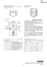
32 31 30 29 28 27 26 25
9
10 11 12 13
TOP VIEW
14 15 16
17
18
19
20
21
22
23
24
8
7
6
5
4
3
2
1
V
OSENSE1
PLLFLTR
PLLIN
FCB
I
TH1
SGND
3.3V
OUT
I
TH2
BOOST1
V
IN
BG1
EXTV
CC
INTV
CC
PGND
BG2
BOOST2
NC
SENSE1
–
SENSE1
+
NC
RUN/SS1
PGOOD
TG1
SW1
V
OSENSE2
NC
SENSE2
–
SENSE2
+
RUN/SS2
TG2
SW2
NC
LTC3728LCUH#TR-R4 (LINEAR)
DUAL, 550KHz, 2-PHASE SYNCHRONOUS STEP-DOWN SWITCHING
REGULATOR
V
OSENSE1
, V
OSENSE2
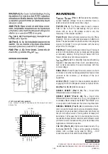
(Pins 1, 9):
Receives the remotely-
sensed feedback voltage for each controller from an
external resistive divider across the output.
PLLFLTR (Pin 2):
The Phase-Locked Loop’s Lowpass
Filter is Tied to This Pin. Alternatively, this pin can be
driven with an AC or DC voltage source to vary the
frequency of the internal oscillator.
PLLIN (Pin 3):
External Synchronization Input to Phase
Detector. This pin is internally terminated to SGND with
50k
Ω
. The phase-locked loop will force the rising top gate
signal of controller 1 to be synchronized with the rising
edge of the PLLIN signal.
FCB (Pin 4):
Forced Continuous Control Input. This input
acts on both controllers and is normally used to regulate
a secondary winding. Pulling this pin below 0.8V will
force continuous synchronous operation.
I
TH1,
I
TH2
(Pins 5, 8):
Error Amplifier Output and Switching
Regulator Compensation Point. Each associated chan-
nels’ current comparator trip point increases with this
control voltage.
SGND (Pin 6):
Small Signal Ground common to both
controllers, must be routed separately from high current
grounds to the common (–) terminals of the C
OUT
capacitors.
3.3V
OUT
(Pin 7):
Output of a linear regulator capable of
supplying 10mA DC with peak currents as high as 50mA.
NC (Pins 10, 16, 29, 32):
No Connect.
SENSE2
–
, SENSE1
–
(Pins 11, 31):
The (–) Input to the
Differential Current Comparators.
SENSE2
+
, SENSE1
+
(Pins 12, 30):
The (+) Input to the
Differential Current Comparators. The I
th
pin voltage and
controlled offsets between the SENSE
–
and SENSE
+
pins
in conjunction with R
SENSE
set the current trip threshold.
RUN/SS2, RUN/SS1 (Pins 13, 28):
Combination of soft-
start, run control inputs and short-circuit detection timers.
A capacitor to ground at each of these pins sets the ramp
time to full output current. Forcing either of these pins
back below 1.0V causes the IC to shut down the circuitry
U
U
U
PI FU CTIO S
required for that particular controller. Latchoff overcurrent
protection is also invoked via this pin as described in the
Applications Information section.
TG2, TG1 (Pins 14, 26):
High Current Gate Drives for Top
N-Channel MOSFETs. These are the outputs of floating
drivers with a voltage swing equal to INTV
CC
– 0.5V
superimposed on the switch node voltage SW.


