1-24
IC
VGN-
S36C/S36GP/S36LP/S36SP/S36TP/S38CP/
S52B/
S62PS/S62PSY/S62S/
S350F/S350FP/
S360/S360P/
S370F
(J/AM
/AO
)
Confidential
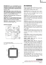
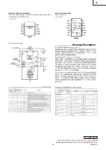
SW2, SW1 (Pins 15, 25):
Switch Node Connections to
Inductors. Voltage swing at these pins is from a Schottky
diode (external) voltage drop below ground to V
IN
.
BOOST2, BOOST1 (Pins 17, 24):
Bootstrapped Supplies
to the Top Side Floating Drivers. Capacitors are connected
between the boost and switch pins and Schottky diodes
are tied between the boost and INTV
CC
pins. Voltage swing
at the boost pins is from INTV
CC
to (V
IN
+ INTV
CC
).
BG2, BG1 (Pins 18, 22):
High Current Gate Drives for
Bottom (Synchronous) N-Channel MOSFETs. Voltage
swing at these pins is from ground to INTV
CC
.
PGND (Pin 19):
Driver Power Ground. Connects to the
sources of bottom (synchronous) N-channel MOSFETs, an-
odes of the Schottky rectifiers and the (–) terminal(s) of C
IN
.
INTV
CC
(Pin 20):
Output of the Internal 5V Linear Low
Dropout Regulator and the EXTV
CC
Switch. The driver and
control circuits are powered from this voltage source. Must
be decoupled to power ground with a minimum of 4.7
µ
F
tantalum or other low ESR capacitor.
EXTV
CC
(Pin 21):
External Power Input to an Internal
Switch Connected to INTV
CC
. This switch closes and
supplies V
CC
power, bypassing the internal
low dropout
regulator, whenever EXTV
CC
is higher than 4.7V. See
EXTV
CC
connection in Applications section. Do not exceed
7V on this pin.
V
IN
(Pin 23):
Main Supply Pin. A bypass capacitor should
be tied between this pin and the signal ground pin.
PGOOD (Pin 27):
Open-Drain Logic Output. PGOOD is
pulled to ground when the voltage on either V
OSENSE
pin is
not within
±
7.5% of its set point.
FU CTIO AL DIAGRA
U
U
W
SWITCH
LOGIC
–
+
0.8V
4.8V
5V
V
IN
V
IN
4.5V
BINH
CLK2
CLK1
0.18
µ
A
R6
R5
+
–
FCB
+
–
–
+
–
+
–
+
V
REF
INTERNAL
SUPPLY
3.3V
OUT
V
SEC
R
LP
C
LP
3V
FCB
EXTV
CC
INTV
CC
SGND
+
5V
LDO
REG
SW
SHDN
0.55V
TOP
BOOST
TG
C
B
C
IN
D
1
D
B
PGND
BOT
BG
INTV
CC
INTV
CC
V
IN
+
C
SEC
C
OUT
V
OUT
D
SEC
R
SENSE
R2
+
+
V
OSENSE
DROP
OUT
DET
RUN
SOFT
START
BOT
TOP ON
S
R
Q
Q
OSCILLATOR
PHASE DET
PLLFLTR
PLLIN
FCB
EA
0.86V
0.80V
OV
V
FB
1.2
µ
A
6V
R1
–
+
R
C
4(V
FB
)
RST
SHDN
RUN/SS
I
TH
C
C
C
C2
C
SS
4(V
FB
)
0.86V
SLOPE
COMP
3mV
+
–
–
+
SENSE
–
SENSE
+
INTV
CC
30k
45k
2.4V
45k
30k
I1
I2
B
DUPLICATE FOR SECOND
CONTROLLER CHANNEL
+
–
–
+
50k
F
IN
+
–
+
–
+
–
+
–
PGOOD
V
OSENSE1
V
OSENSE2
0.86V
0.74V
0.86V
0.74V
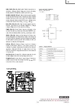
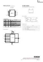
M24C02-WDW6TP (STMICRO)
SERIAL I
2
C BUS EEPROM
– TOP VIEW –


