1-19
IC
VGN-
S36C/S36GP/S36LP/S36SP/S36TP/S38CP/
S52B/
S62PS/S62PSY/S62S/
S350F/S350FP/
S360/S360P/
S370F
(J/AM
/AO
)
Confidential
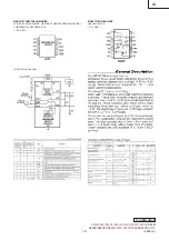
LM2729SQX (NATIONAL SEMICONDUCTOR)
TWO-PHASE CURRENT-MODE HYSTERETIC BUCK CONTROLLER FOR
PROCESSORS REQUIRING IMVP-IV
SG
ND
V
B
OOT
VDPSLP
VDPRSLP
VI
D4
DPSLP#
DPRSL
P
VR_O
N
VREF
VDAC
VI
D5
P_Z1
1
2
3
4
5
6
8
7
9
10
11
12
CM
P1
CM
PREF
DG
ND
SYNC2
VDD
SYNC1
VO
VP
CM
P2
OU
T
2
OU
T
1
IL
IM2
IL
IMR
E
F
36
35
34
33
32
31
29
30
28
27
26
25
SS
MCH_OK
NC
SENSE
CLK_EN#
V1R7
NC
VID1
PSI#
VID2
VID0
TGND
VID3
NC
NC
ILIM1
PGND1
SW1
P_Z0
PGOOD
38
39
40
41
42
43
44
45
46
47
23
22
21
20
19
18
17
16
15
14
NC
NC
13
24
NC
NC
37
48
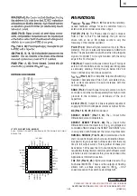
Top View
48-Lead LLP (SQA)
Pin Descriptions
(SQA48A, non-pullback)
Pin 1, VID4
: One of the six logic VID pins to program the output
voltage.
Pin 2, VID5
: One of the six logic VID pins to program the output
voltage. This is the MSB pin.
Pin 3, DPSLP#
: When this pin is logic low, VREF voltage is equal
to that on the VDPSLP pin.
In an IMVP-IV solution, this pin
should be connected to the STP_CPU# signal to support the
Deep Sleep mode.
Pin 4, DPRSLP
: When this pin is logic high, VREF voltage is
equal to that on the VDPRSLP pin. In an IMVP-IV solution, this
pin should be connected to the DPRSLPVR signal to support the
Deeper Sleep mode.
Pin 5, VR_ON
: Chip enable input. This pin should be connected
to the VR_ON signal specified in the IMVP-IV document.
Pin 6, VREF
: Desired regulator output voltage under no load.
Pin 7, VDPRSLP
: Desired Deeper Sleep mode output voltage, as
specified in the IMVP-IV document. Connect this pin to the de-
sired reference level.
Pin 8, VDPSLP
: Desired Deep Sleep mode output voltage, as
specified in the IMVP-IV document. Connect this pin to the de-
sired reference level.
Pin 9, VBOOT
: Initial output voltage desired after soft start com-
pletes, as specified in the IMVP-IV document. Connect this pin to
the desired reference level.
Pin 10, SGND
: Signal ground.
Pin 11, VDAC
: Buffered Digital-to-Analog converter output.
Pins 12, P_Z1
: Reference adjust, do not connect.
Pins 13, NC
: No connect.
Pins 14, NC
: No connect.
Pins 15, P_Z0
: Reference adjust, do not connect.
Pin 16, TGND
: Reserved for test purpose. Must be connected to
signal ground.
Pin 17, V1R7
: 1.7V reference voltage.
Pin 18, SS
: Soft start, soft shutdown and slew rate control. Con-
nect a capacitor between this pin and ground to control the soft
start and soft shutdown speed. The value of the capacitor will
also define the slew rate of the SpeedStep
¥
transitions.
Pin 19, PGOOD
: Power good flag. Goes open-drain when output
voltage enters the power good window and MCH_OK is asserted.
Masked during transitions. See Timing Diagram for further de-
tails.
Pin 20, MCH_OK
: only when this pin is a logic high can PGOOD
pin be pulled high. This pin should be connected to the PGOOD
pin of the LM2728 in an IMVP-IV solution.
The corresponding
signal is the MCH_PWRGD in the IMVP-IV document.
Pin 21, SENSE
: Regulator output voltage sense.
Connect di-
rectly to output.
Pin 22, CLK_EN#
: Signal to start clock chip PLL locking. This is
the CLK_ENABLE# signal specified in the IMVP-IV document. It
goes low when asserted.
Pins 23, NC
: No connect.
Pins 24, NC
: No connect.
Pin 25, VOVP
: Over-voltage protection level. Connect this pin to
the desired reference voltage to set the trigger level for over-
voltage protection.
Pins 26, CMPREF
: Inductor current reference. Voltage between
this pin and the regulator output determines the inductor current.
Pin 27, CMP2
: Current sense for Channel 2. Voltage between
this pin and the regulator output sets the inductor current.
Pin 28, CMP1
: Current sense for Channel 1. Voltage between
this pin and the regulator output sets the inductor current.
Pin 29, SYNC2
: Connect to the SYNC pin of the LM2724 to en-
able or disable the turning on of the bottom power FET.
Pin 30, OUT2
: Channel 2 pulse output to control the switching of
the external MOSFET driver such as the LM2724.
Pin 31, DGND
: Digital ground.
Pin 32, VDD
: Chip power supply.
Pin 33, OUT1
: Channel 1 pulse output to control the switching of
the external MOSFET driver such as the LM2724.
Pin 34, SYNC1
: Connect to the SYNC pin of the LM2724 to en-
able or disable the turning on of the bottom power FET.
Pin 35, ILIMREF
: Current limit reference. Voltage between this
pin and the regulator output sets the indutor current limit level.
Pin 36, ILIM2
: Current limit sense for Channel 2.
Voltage be-
tween this pin and the regulator output is the voltage across the
current sense resistor.
Pins 37, NC
: No connect.
Pins 38, NC
: No connect.
Pin 39, ILIM1
: Current limit sense for Channel 1.
Voltage be-
tween this pin and the regulator output is the voltage across the
current sense resistor.
Pin 40, PGND1
: Connect to Channel 1 bottom FET source node
(ground) to detect negative inductor current.
Pin 41, SW1
: Connect to Channel 1 switch node (drain of bottom
power FET) to detect negative inductor current.
Pin 42, PSI#
: Power saving mode trigger signal.
Pin 43, VID0
: One of the six logic VID pins to program the output
voltage. This is the LSB pin.


