


7-5
4. Overall Level Characteristic and Distortion Factor
Check
Purpose:
Check the record level, play level, and distortion factor against the
reference input.
Mode
REC and PB (SP mode)
Signal
400 Hz, –7.5 dBs
Measurement point
Audio output terminal
Measurement equipment
Audio level meter and
distortion factor meter
Specified value
Playback level: –7.5 ± 4.0 dBs
Distortion factor: 4% or less
Confirmation Method:
1) Supply an audio signal of 400 Hz, –7.5 dBs simultaneously to
both L and R channels of Audio Line Input.
2) Make recording
3) Play back a recorded portion.
4) Confirm that a playback level is –7.5 ± 4.0 dBs. (mono audio)
5) Confirm that a distortion factor is less than 4%.
5. Overall S/N Check
Purpose:
Confirm that the S/N is within the specification.
Mode
REC and PB (SP mode)
Signal
Short
Measurement point
Audio output terminal
Measurement equipment
Audio noise meter
Specified value
–46.0 dBs or less
Confirmation Method:
1) Connect both L and R channels of audio line input to the GND.
2) Start recording.
3) Play the recorded part to confirm that the noise is below –46.0
dBs.
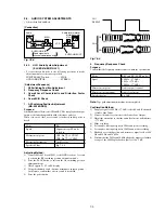
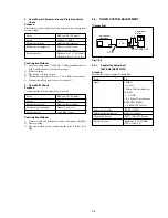
2-5.
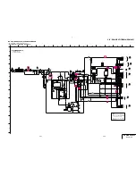
TUNER SYSTEM ADJUSTMENT
[Connection]
Fig. 7-2-6
2-5-1.
Separation Adjustment
(SLV-ED818/ED919TW)
Purpose:
Mixed audio signal separate Lch and Rch.
Mode
E-E
Signal
VIDEO:
color bar
(White 100% modulation)
AUDIO:
L NONE
R 1 kHz 60% modulation
ELECTRIC FIELD:
60–80 dBs/75
Ω
Term
Measurement point
Pin
qx
of IC701
Measurement equipment
Audio level meter
Adjusting Element
RV701 (MA-402 Board)
Specified value
minimum -9.9 ± 0.2 dBm
(700 ± 14mVp-p)
47 k
Ω
VCR
Audio level
meter
Up channel
convertor
RF IN
AUDIO LINE OUT
L
R
Содержание RMT-V310
Страница 24: ...SLV ED212 ED717 ED818 ED919 LF1 3 1 3 2 SECTION 3 BLOCK DIAGRAMS 3 1 OVERALL BLOCK DIAGRAM ...
Страница 27: ...SLV ED212 ED717 ED818 ED919 LF1 3 4 AUDIO BLOCK DIAGRAM 3 7 3 8 ...
Страница 28: ...SLV ED212 ED717 ED818 ED919 LF1 3 5 TUNER BLOCK DIAGRAM 3 9 3 10 ...
Страница 29: ...SLV ED212 ED717 ED818 ED919 LF1 3 6 MODE CONTROL BLOCK DIAGRAM 3 11 3 12 ...
Страница 30: ...SLV ED212 ED717 ED818 ED919 LF1 3 7 POWER BLOCK DIAGRAM ED212 ED717 ED919KR LF1 ED818 ED919TW 3 13 3 14E ...


