1-3.
Circuit Description
1-3-1.
CMOS Block and Lens Block
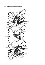
BI-202A/203A/204A Boards
The BI-202A/203A/204A Boards are used to supply the power bias and synchronous signal to the CMOS image sensor
(ICl) and to transmit output signals to the DCP-56 board through the HN-399 board. This board is provided with a 80-
pin B to B connector (CN1) for transmission of video signals and power.
The CMOS image sensor converts optical signal to electrical signal, and its internal A/D converter converts the electrical
signal to 12-bit digital signal and outputs the digital signal. Video signals are used for the R channel on the BI-202A
board, the G channel on the BI-203A board, and the B channel on the BI-204A board.
This board is also provided with functions as an electronic shutter and an analog gain amplifier. The sync signal and the
serial communication signal from the DCP-56 board are input to the CMOS image sensor.
Various types of decoupling capacitors and damping resistors are also mounted on this board.
The temperature sensor (IC3) of the BI-203A board sends the temperature data to the camera microcomputer SUN
(IC702) on the DCP-56 board through the I
2
C bus.
The drop regulator (IC2) in the power supply circuit supplies smoothed power voltages to the CMOS image sensor.
1-3-2.
Camera Block
DCP-56 Board
The camera block consists of a camera signal processor IC that processes the digital camera signal and a camera
microcomputer that controls the camera signal processor IC, CMOS image sensor, and lens. This block outputs the
digital video signal (Y/C) to the following video signal system (baseband).
The digital video signal sent from the HN-339 board is input to the camera signal processor (IC200: RISE) on the DCP-56
board. The camera signal processor detects values (including video signal average value and peak value) necessary for
the camera operations such as white balance, black balance, focus, iris, knee processing, and then sends the detected
values to the camera microcomputer SUN (IC702).
The digital video signal enters first the selector circuit that selects digital video signal or the test signal, and is then
transferred to the CMOS image sensor correction circuit and the lens correction circuit.
After that, the digital video signal receives white balance processing, and then the matrix signal and the detail signal are
added to the video signal. The video signal then receives pedestal control, knee correction, gamma correction, and white/
black clip processing. The video signal is finally output to the baseband processing IC T-ONE (IC900) .
The processing for converting the number of pixels from 1920/1080 to 1440/1080 or from 1920/1080 to 1280/720 is
also performed in the camera signal processor IC RISE (IC200).
The camera microcomputer SUN (IC702) performs the overall camera control, and is controlled by the system
microcomputer (IC2101: MELON) on the DPR-343 board. SUN's peripheral ICs FLASH ROM (IC701) and SDRAM
(IC700) are mounted on the DCP-56 board.
1-3-3.
Video Signal System
DCP-56 Board
The digital video signal (Y/C) sent from the camera signal processor IC RISE (IC200) on the DCP-56 board is input to
the baseband processing IC T-ONE (IC900).
The baseband processing IC T-ONE that incorporates scaler functions (supporting multi-format output), OSD, PLL (54
to 74 MHz), and CPU performs baseband processing for video and audio signals.
PMW-200/PMW-EX280
1-5
Содержание PMW-200
Страница 1: ...SOLID STATE MEMORY CAMCORDER PMW 200 PMW EX280 SERVICE MANUAL 1st Edition Revised 1 ...
Страница 4: ......
Страница 8: ......
Страница 10: ......
Страница 30: ......
Страница 38: ...3 Install the removed parts by reversing steps of removal PMW 200 PMW EX280 2 8 ...
Страница 82: ......
Страница 96: ......
Страница 122: ...Lens Block Assembly 1301 No Part No SP Description 1301 A 1911 477 A s FRONT ASSEMBLY RP PMW 200 PMW EX280 5 16 ...
Страница 128: ......
Страница 130: ......
Страница 132: ......
Страница 133: ......


