background image

43

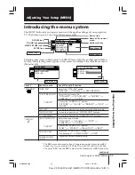
Adjusting Your Setup (MENU)

Sony KP-FX53/FX43  M61 (

GB

/FR/CT/CS/PR/AR).4-090-470-

21 

(1)

Note

• If “ECO MODE” is on, the ECO MODE (

 ) icon will appear at the

bottom right corner of the screen when you turn on the projection TV or
when you press 

 on the remote.

To return to the normal screen

Press MENU.

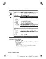
Select

“CONVERGENCE”

“CH PRESET”

“PROGRAM
SETUP”

“COL SYS”

“ECO MODE”

To

adjust the convergence.

CONVERGENCE

DIGITAL QUICK FOCUS

MANUAL ADJUST

You can select automatic or manual convergence adjustment.
See “Adjusting the convergence manually” on page 44.

preset channels.

CH PRESET

AUTO PROGRAM

MANUAL PROGRAM
TV SYS : B/G

You can select automatic or manual channel presetting.
See “Presetting channels manually” on page 45.
You can change the TV system by selecting “TV SYS”.

skip unwanted channels, or block channels.

PROGRAM SETUP

PROG :

 09

SKIP : OFF
CHILD LOCK : OFF 

See “Skipping unwanted or unused channels” and “Blocking
channels”, respectively.

select the color system. Normally, set this to “AUTO”.
You can select the color system for each channel or each video input.

reduce power consumption of your projection TV to save energy.
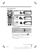
Move 

 up or down to select “ON”, then press 

.

To cancel, select “OFF”, then press 

.

continued

01GB09ADJ-p65

02.8.21, 5:24 PM

43

Содержание KP-FX43M31

Страница 1: ...AUS SCC P95D A KP FX43M61 RM 998 GE SCC P90D A KP FX43M91 RM 998 ME SCC P94D A RM 998 KP FX43M31 M61 M91 KP FX53M31 M61 M91 KP FX53M31 RM 998 AUS SCC P95C A KP FX53M61 RM 998 GE SCC P90C A KP FX53M91 RM 998 ME SCC P94C A TV VIDEO DRC MF HD DVD 1 2 3 4 5 6 7 8 0 9 JUMP PROG OPTION RESET A B PROG INDEX MENU TWIN PROG TWIN PROG ...

Страница 2: ...CATV S01 to S03 S1 to S41 VHF C1 to C12 R1 to R12 UHF C13 to C57 R21 to R60 CATV S01 to S03 S1 to S41 Z1 to Z39 VHF A2 to A13 UHF A14 to A79 CATV A 8 to A 2 A to W 4 W 6 to W 84 75 ohm external terminal 15W 15W 10 distortion Input 4 Output 1 Phono jacks 1 Vp p 75 ohms Input 4 Output 1 Phono jacks 500 mVrms Input 2 Y 1 Vp p 75 ohms unbalanced sync negative C 0 286 Vp p 75 ohms Input 2 Phono jacks Y...

Страница 3: ... with Commander 19 3 10 1 How to Select Each Mode 19 3 10 2 How to Enter Service Mode 19 3 10 3 Method of Cancellation from Service Mode 20 3 10 4 How to Adjustments 20 3 10 5 How to Write the Data 20 3 10 6 Memory Write Confirmation Method 20 TABLE OF CONTENTS 3 11 Service List 21 3 12 Registration Adjustment 3 12 1 Adjustment Flow 49 3 12 2 Setup for Adjustment 49 3 12 3 Method of Main Deflectio...

Страница 4: ... 7 EXPLODED VIEWS 7 1 Front Panel Block 174 7 2 Cabinet Block KP FX53 175 7 3 Cabinet Block KP FX43 176 7 4 Bezenet and Mirror Cover Block KP FX53 177 7 5 Bezenet and Mirror Cover Block KP FX43 178 7 6 Main Braket and Picture Tube Block 179 8 ELECTRICAL PARTS LIST 180 ...

Страница 5: ... the possible cause of the problem If there is more than one error the lamp will identify the first of the problem areas Result for all of the following diagnostic items are displayed on screen No error has occurred if the screen displays a 0 002 000 or 002 001 255 003 000 or 003 001 255 004 000 or 004 001 255 005 000 or 005 001 255 006 000 or 006 001 255 007 000 or 007 001 255 101 000 or 101 001 ...

Страница 6: ...rom the outlet to stop the STANDBY TIMER lamp from flashing Diagnostic Item Flash Count B overcurrent 2 times B overvoltage 3 times V deflection stop 4 times White balance failure 5 times High voltage protector 6 times Audio Protection 7 times One flash count is not used for self diagnostic STANDBY TIMER lamp Lamp ON 0 3 sec Lamp OFF 0 3 sec Lamp OFF 3 sec 2 times 3 times 5 times 6 times 4 times 7...

Страница 7: ...k the self diagnostic screen SELF DIAGNOSTIC 002 000 003 000 004 000 005 001 006 002 007 000 101 000 Numeral 0 means that no fault has been detected Numeral 1 means a fault has been detected Numeral 2 means two faults have been detected during repairs When you have completed the repairs clear the result display to 0 Unless the result display is cleared to 0 the self diagnostic function will not be...

Страница 8: ... or become low level within 5 seconds This error will be detected by IC4300 TV will stay on but there will be no picture High voltage or Horizontal Deflection Protect Occurs when an overvoltage of horizontal pulse is detected by D8038 and IC8006 If the voltage of pin 1 of IC8006 goes to High the voltage to pin 57 of IC4300go to UP The unit will automatically turn off Audio Protector If the Audio o...

Страница 9: ... plier or the like from chassis assembly in case of checking printed circuit boards After checking turn over the covers and secure them with screws screws 7 685 648 79 BVTP 3X12 1 Eleven screws Hexagon head 2 Rear board 1 Eleven screws Hexagon head 2 Rear board 3 Main bracket section 1 Optical shield 2 Two screws tapping screw hexagon head 1 Main bracket section 2 Eight screws BVTP 3X12 ...

Страница 10: ...g screw hexagon head 2 Three screws tapping screw hexagon head 5 Side panel 43R assy 2 Three screws tapping screw hexagon head 4 Side panel 43L assy 3 Two screws tapping screw hexagon head 2 Three screws tapping screw hexagon head 1 Three screws BVTP 4x16 1 three screws BVTP 4x16 3 Two screws tapping screw hexagon head 2 Three screws tapping screw hexagon head 5 Side pane 53R assy 6 Front panel 43...

Страница 11: ...Front panel assy 9 H3 board 8 Four screws BVTP 3x12 2 Four screws BVTP 4X16 2 Six screws BVTP 4X16 1 Two screws Hexagon head 2 Four screws BVTP 4X16 4 Mirror cover 1 Four screws Hexagon head 8 Screen holder SIDE 7 Screen holder SIDE 6 Screen holder TOP 9 Screen holder LOW 5 Six screws BVTP 4X16 5 Four screws BVTP 4X16 5 Twelve screws BVTP 4X16 Holder Bracket 43R Diffusion plate F Diffusion plate L...

Страница 12: ... Two screws Hexagon head 2 Two screws Hexagon head 2 Six screws BVTP 4X16 3 Mirror cover 2 Six screws BVTP 4X16 1Four screws Hexagon head 8 Screen holder SIDE 7 Screen holder SIDE 6 Screen holder TOP 9 Screen holder LOW 5 Six screws BVTP 4X16 5 Four screws BVTP 4X16 5 Twelve screws BVTP 4X16 Diffusion plate F Diffusion plate L Contrast screen 3 Six screws Hexagon head 0 Beznet assy 2 Main bracket ...

Страница 13: ...KP FX53M31 M61 M91 RM 998 2 8 G BOARD REMOVAL 2 9 CONNECTOR COVER REMOVAL 1 Three holder PWB Main bracket section 2 G board 3 Connector cover section Main bracket section 1 Tow screws BVTP 4X16 2 Screw PSW 2 6X6 RF Connector ...

Страница 14: ...FX43M31 M61 M91 KP FX53M31 M61 M91 RM 998 2 10 J BOARD REMOVAL 2 11 A1 E B4 AND V2 BOARDS REMOVAL 3 Four screws BVTP 3X12 5 Connector cover 4 J board 2 J board cover 1 A1 board 2 E board 3 B4 board 4 V2 board ...

Страница 15: ...URE TUBE REMOVAL 1 A board 4 D board 3 Five screws BVTP 3X12 2 AD board 6 Main bracket section 4 Picture tube block assy 2 Three screws Hexagon head 4X20 2 Three screws Hexagon head 4X20 5 Two screws Hexagon head 4X20 1 Two screws BVTP 4X16 1 Three screws BVTP 4X16 3 Three screws BVTP 4X20 ...

Страница 16: ...strictly inhibited If removed it may cause liquid spill 6 Mechaseal assy R 4 Deflection yoke 7 Extension spring 8 Plate shading Green Red only 9 Cushion Geen Red only 5 Four screws BVTP 4X16 1 When installing the Machaseal assy RED and GREEN be sure to reuse the Plate shading 2 Check alignment to make sure the Plate shadings are the right positions as following Fig 2 5 2 Rubber cap 1 HV cable Hook...

Страница 17: ...and align the tilt of the Deflection yoke so that the bars at the center of the monoscope pattern are horizontal 4 After aligning the deflection yoke fasten it securely to the funnel shaped portion of the CRT 5 The tilt of the deflection yoke for red and blue is aligned the same as was done for green Fig 3 6 4 Pole Magnet Make sure deflection yoke is touching CRT closely Anode cap 2 Pole Magnet De...

Страница 18: ...ix lens screw 5 Repeat above process for red and blue 6 Rotate the blue lens and adjust to obtain the best lens focus at the both side area 7 Fix blue lens screw 3 9 2 Green and Red Dot Hatch Electrical Focus Adjustment 1 Receive the signal 2 Place the caps on the red and blue lens so that only the green color is shown 3 Rotate the green focus VR on the focus pack and adjust to obtain the best ele...

Страница 19: ...o return to normal screen 4 Selection of TWIN mode 1 Press TWIN button on the commander 2 Press TWIN button again to return to normal screen 5 Selection of INDEX mode 1 Press PROGR INDEX button on the commander 2 Press PROGR INDEX button again to return to normal screen 3 10 2 How to Enter Service Mode 1 Turn on the main power switch to place this set in standby mode LED will light in red 2 Press ...

Страница 20: ... READ Reads data from NVM 8 NORMAL All user control goes to the standard 5 INITIAL Service data initialization Not stored Be sure not to use usually 2 COPY Do not operate with a remote commander WRT5060 The data vary with among mode Note Before changing to other modes press MUTE buttons on the commander to write the data Omission of this operation causes the data to be returned to the data before ...

Страница 21: ...9 04 MPN HORIZONTAL MIDDLE PIN 00 00 00 00 00 00 00 00 00 05 PIN HORIZONTAL PIN 01 01 01 01 01 01 01 01 01 06 PN0 PIN OFF SET PJ only 07 07 07 07 07 07 07 07 07 07 UCP UPPER CORNER PIN 1F 1F 1F 1F 1F 1F 1F 1F 1F 08 LCP LOWER CORNER PIN 1F 1F 1F 1F 1F 1F 1F 1F 1F 09 UXG UPPER EXTRA CORNER PIN GAIN 00 00 00 00 00 00 00 00 00 0A LXG LOWER EXTRA CORNER PIN GAIN 00 00 00 00 00 00 00 00 00 0B UXP UPPER ...

Страница 22: ... 00 00 00 00 00 00 10 LVL LOWER VERTICAL LINEARITY 00 00 00 00 00 00 00 00 00 00 GE2 00 HCT HORIZONTAL CENTERING 13 13 13 13 13 13 13 13 13 13 01 HPS HORIZONTAL POSITION 17 17 17 17 17 17 17 17 17 17 02 HSZ HORIZONTAL SIZE 1F 1F 1F 1F 1F 1F 1F 1F 1F 1F 03 SLN HORIZONTAL S CORRECTION 09 09 09 09 09 09 09 09 09 09 04 MPN HORIZONTAL MIDDLE PIN 00 00 00 00 00 00 00 00 00 00 05 PIN HORIZONTAL PIN 01 01...

Страница 23: ...D PIN DC LEVEL SHIFT 00 00 00 00 00 00 00 00 00 10 AKT AKB TIMING 16 16 09 09 09 10 16 16 09 11 PPL PIN COMP POLARITY 00 00 00 00 00 00 00 00 00 12 M15 FH 15K MS MODE 00 00 00 00 00 00 00 00 00 13 HFQ Fh setting multi scan 50 50 50 50 50 50 50 50 50 14 HFX Reciprocal Fh mult scan 19 19 19 19 19 19 19 19 19 15 VMP VERTICAL MULTI SCAN MODE 00 00 00 00 00 00 00 00 00 16 ITL FREERUN INTERLACE SETTING ...

Страница 24: ...N DC LEVEL SHIFT 00 00 00 00 00 00 00 00 00 00 10 AKT AKB TIMING 10 10 09 12 12 10 09 09 09 09 11 PPL PIN COMP POLARITY 00 00 00 00 00 00 00 00 00 00 12 M15 FH 15K MS MODE 00 00 00 00 00 00 00 00 00 00 13 HFQ Fh setting multi scan 50 50 50 50 50 50 50 50 50 50 14 HFX Reciprocal Fh mult scan 19 19 19 19 19 19 19 19 19 19 15 VMP VERTICAL MULTI SCAN MODE 00 00 00 00 00 00 00 00 00 00 16 ITL FREERUN I...

Страница 25: ...or Cr Signal 1F 1F 29 29 1F 29 29 1F 03 SBR Sub Brightness Control 1F 04 RDR R Drive 1F 05 GDR G Drive 17 06 BDR B Drive 1F 07 RCT R Cutoff 1F 08 GCT G Cutoff 1B 09 BCT B Cutoff 1F 0A SBO Sub Brightness Offset 1F 0B RDO R Drive Offset 1F 0C GDO G Drive Offset 1F 0D BDO B Drive Offset 1F 0E RCO R Cutoff Offset 1F 0F GCO G Cutoff Offset 1F 10 BCO B Cutoff Offset 1F RGB Others MS Category Item Functi...

Страница 26: ...46 0B 53 04 46 07 53 0B 46 0E 53 08 46 0B 53 08 46 0B Standard Data Category Item Function Common 50 60 50 60 Input Node Table Group 2 Twin Index YUV RGB OTHER MS No Name TV VIDEO TV VIDEO SD I SD P HD SD I SD P HD SAJ 00 PIC Picture Control 1 01 BRT Brightness Control 1 02 COL Color Control 1 03 HUE Hue Control 1 04 SHP Sharpness Control 1 05 VML VM Level 1 06 DYC Dynamic Color on off 1 07 WBS Wh...

Страница 27: ...5 ENS Environmental SW 06 TES Temperature SW 07 NSS NS SW 08 EWS EW SW 09 NSG NS Correction Gain 0A EWG EW Correction Gain 0B ENG Environmental Correction Gain 0C ENS NS Correction by Environment 0D TLD Temp Corr DC of Left side 0E TLU Temp Corr DC of Left side 0F TLL Temp Corr Gain of Left Upper 10 TRD Temp Corr Gain of Left Lower 11 TRU Temp Corr Gain of Right Upper 12 TRL Temp Corr Gain of Righ...

Страница 28: ... 03 0B LTI Luminance Transient Improvement 02 02 00 02 0C LTM LTI Mode Setting 01 0D CTI Chrominance Transient Improvement 01 01 00 01 0E VDL VM OUT Phase Control 08 07 0A 07 07 07 0F 07 07 0F 07 0F VCR VM OUT Coring Level Setting 00 00 00 00 00 00 00 00 00 00 00 10 VFO VM OUT F0 Setting 02 02 02 02 02 02 02 02 02 02 02 11 VLM VM OUT Limiter Level Setting 03 03 03 03 03 03 00 03 03 00 00 12 SPH H ...

Страница 29: ... Cr LPF Switch 01 11 YDL Y DL Time Adjustment 06 05 05 03 12 B01 Cb Offset1 Adjustment main route 0A 13 RO1 Cr Offset1 Adjustment 07 14 CDF V Count Down Frequency Switch 00 15 CDM V Count Down Judge Switch 00 16 AFC AFC Sensitivity Switch 00 00 17 MVM Macrovision Mask AFC Mask 00 18 SRY SECAM R Y Black Adjustment 07 19 SBY SECAM B Y Black Adjustment 01 1A BEL SECAM BELL HPF Switching 02 1B BLF BEL...

Страница 30: ... 02 0E FSW BPF TQF Switch 01 0F SDT SECAM Double Trap Switch 01 10 LPF Y Cb Cr LPF Switch 01 11 YDL Y DL Time Adjustment 05 03 03 03 12 NCM 1 H Addition Switch 01 13 B01 Cb Offset1 Adjustment main route 07 14 RO1 Cr Offset1 Adjustment 07 15 CDF V Count Down Frequency Switch 00 16 CDM V Count Down Judge Switch 00 17 AFC AFC Sensitivity Switch 00 1F 00 18 MVM Macrovision Mask AFC Mask 00 19 SRY SECA...

Страница 31: ...nc Separation Mode 01 08 HTC H Sync Separation Time Constant 01 00 09 HSW YG Out signal Output 00 0A HMA Hsync within V sync 00 0B MAC Macrovision 01 0C DUM Out dummy sync or signal sync 00 0D CLK Clock Select 00 0E GSL Gain Select 00 0F CBG CB Gain 07 10 CRG CR Gain 07 11 YG Y Gain 07 12 HFR Dummy Frequency Select 01 Standard Data Function Category Item Table Input Siganl fh15k 525i 625i otherfh ...

Страница 32: ...W G Agreement Count 01 04 WDL W G Search Delay 30 05 NDL NICAM Search Delay 20 06 SDL Stereo status Read Delay 10 07 AGC AGC Switch Auto Constant 01 08 REL AGC Gain at Constant Mode 28 09 CRM Carrier muting on off 00 0A ACO Audio Clock out on off 01 0B FP FM Prescale for non M system 1B 0C FPM FM Prescale for M system 32 0D FH FM Prescale for HDEV 36 0E FHM FM Prescale for HDEV and M 65 0F WGP W G...

Страница 33: ...BL Blue Stretch Switch 00 12 GBL Blue Stretch Gain Selection 00 13 SBL Blue Stretch Size selection 00 14 CDS Color Dependent Sharpness 01 01 01 01 15 CST Threshold of Color Dependent Sharpness 07 16 CTI Color Transient Improvement 00 00 00 00 17 BON Black offset Compensation 00 00 00 00 18 BTD Adaptive Black Strecth 00 00 00 00 19 NLD Non Linearity Amplifier 00 1D 13 05 13 1A NLW Step Width of Non...

Страница 34: ...dth 05 VPW display v pulse width 06 YCD display output yc signal delay correct 07 YSD display output ys signal delay correct 08 MHP main display picture h position 09 MVP main display picture v position 0A MHS main display picture h size 0B MVS main display picture v size 0C MPH multi picture mode h position 0D MPV multi picture mode v position 0E SHP sub display picture h position 0F SVP sub disp...

Страница 35: ...Pr RF CV S Video YPbPr RF CV S Video YPbPr RF CV S Video YPbPr 00 HAP A1 A0 B2 B1 84 83 95 94 84 83 95 94 01 HAS A2 A2 9F 9F B2 B2 AF AF B2 B2 AF AF 02 VAP 24 24 30 30 29 29 35 35 24 24 30 30 03 VAS 78 78 90 90 6E 6E 84 84 78 78 90 90 Item Standard Data No Name Twin Left Scroll Index Main 60Hz 50Hz 60Hz 50Hz RF CV S Video YPbPr RF CV S Video YPbPr RF CV S Video YPbPr RF CV S Video YPbPr 00 HAP 95 ...

Страница 36: ...z 50Hz 480i RF CV S Video 480p 1080I 720p 576i RF CV S Video 576p 1080i 720p 08 PSP 3E 81 8B BA 4D 9B 8B BA 09 PST 0 0 0 0 0 0 0 0 MD3 Standard Data 3 No Name MD3 00 HAP VDO H Active Area Position 01 HAS VDO H active Area pixel size 02 VEP VDO V active even position 03 VLS VDO V active area line size 04 VOP VDO V active odd position 05 CLM VDO Clamp pulse output timing 06 CPW VDO Clamp pulse width...

Страница 37: ... coring code 11 MVL Main V enhance c cliping code 12 MVE Main V enhance c level code 13 SHY sub h LPF y coefficient Code 14 SHC sub h LPF c coefficient Code 15 SVY sub v LPF y coefficient Code 16 SVC sub v LPF c coefficient Code 17 SHR sub h enhance y coring code 18 SHL sub h enhance y cliping code 19 SHE sub h enhance y level code 1A SHO sub h enhance y coefficient code 1B SCR sub h enhance c cor...

Страница 38: ...3 2 1 1 3 2 10 MVR 2 2 0 2 2 2 0 2 2 2 2 2 2 2 2 2 11 MVL 1 1 0 1 1 1 0 1 1 1 1 1 1 1 1 1 12 MVE 0 0 0 0 0 0 0 0 0 0 0 0 0 0 0 0 53 3 43 1 53 1 43 0 Item Standard Data No Name POP 10 POP 11 POP 12 POP 13 POP 14 POP 15 POP 16 POP 17 POP 18 POP 19 POP 1A POP 1B POP 1C POP 1D POP 1E POP 1F 576i Component 480i Component 576i Composite Normal Mode Wide model only 480i RF Composite Normal Mode Wide mode...

Страница 39: ...1 1 0 1 3 1 1 0 1 3 3 0 3 3 3 0 3 10 MVR 2 2 0 2 2 2 0 2 0 0 0 0 0 0 0 0 11 MVL 1 1 0 1 1 1 0 1 0 0 0 0 0 0 0 0 12 MVE 0 0 0 0 0 0 0 0 0 1 0 1 0 1 0 1 Item Standard Data No Name POP 30 POP 31 POP 32 POP 33 POP 34 POP 35 POP 36 POP 37 POP 38 POP 39 POP 3A POP 3B POP 3C POP 3D POP 3E POP 3F 1080i 50 60Hz 720p 50 60Hz P P Index Scroll Memory Stick Dynamic Standard Hi Fine Personal Dynamic Standard Hi...

Страница 40: ...Standard Data 1 No Name MD6 00 MCT Main Cut Out on 01 MWH Main Write H size 02 MWV Main Write V size 03 MHP Main Read H position 04 MVP Main Read V Position 05 MHS Main Read H Size 06 MVS Main Read V Size MD7 00 MCN Main Contrast 01 SCR Sub Contrast R 02 SCG Sub Contrast G 03 SCB Sub Contrast B 04 RGB RGB OUT Select Category Standard Data Function Functionality 0 1 1 1 1 1 ...

Страница 41: ... ON OFF 00 0C VBL V H Blanking level adjustment 00 0D UBL U H Blanking level adjustment 00 0E CDL U V output delay 00 00 0F YDL Y output delay 00 00 10 PVI VD input polarity 00 11 PHI HD input polarity 00 12 HDW HD pulse width 10 13 PVO VD output polarity 00 14 PHO HD output polarity 00 15 HST HD out pulse start position 36 16 VDL VD out Pulse start position 00 17 VDW VD out Pulse width 03 18 NDE ...

Страница 42: ...03 03 2C YLM Y NR Feed back limit level 00 03 04 08 02 03 04 08 2D CLV C NR level 00 08 09 0B 04 08 09 0B 2E CNT Relate C NR to YSTDN 01 2F CPL Relate C NR to YSTDP 01 30 CMG C Moving detection gain 00 00 00 00 00 00 00 00 31 CCR C Moving detection level 00 00 06 0C 00 00 06 0C 32 CLM C NR Feed back limit level 00 04 05 05 00 04 05 05 33 NVS NR Vertical start line 14 14 34 NHS NR Horizontal start ...

Страница 43: ...ync Non standard 01 01 13 LDR Sensitivity Selection for Frame sync Non standard 02 01 14 VAP Gain Adjustment for Vertical Shape Correction 00 00 00 00 15 VAI Vanishing Adjustment for Vertical Shape Correction 00 00 00 00 16 YPF Center Frequency Selection for Y peaking BPF 03 03 03 03 17 YPG Gain Adjustment for Y peaking BPF 0A 08 08 08 18 VSE Line Comb Filter Setup 02 19 CCN C signal Split Filter ...

Страница 44: ...7 02 THD Teletext H sync Active Edge Shift 00 03 TVD Teletext V sync Active Edge Shift 00 04 HPL Teletext H sync Polarity Configuration 01 05 VPL Teletext V sync Polarity Configuration 00 06 FPL Teletext V sync Polarity Configuration 01 07 FMD Teletext Fastext TOP Force Mode 02 08 TBR Teletext RGB Brightness 03 09 NOP 02 M91 Teletext National Option Table Configuration 01 M31 M61 02 M91 01 M31 M61...

Страница 45: ...27 127 127 127 127 19 DFV1 V1 saw wave for dynamic focus 128 127 60 50 60 50 20 50 20 50 50 40 40 40 90 50 90 50 40 50 40 50 20 SDHP Compensation of horizontal phase for shading 0 4095 500 21 SDH1 Horizontal saw wave for shading 4 3 128 127 63 127 127 127 63 127 127 127 63 127 63 127 63 127 127 127 63 127 127 127 22 BDVU Vartical positioni for boder line 1 0 2047 6 4 4 0 11 9 7 0 45 41 45 41 10 8 ...

Страница 46: ...4 SZLM Size Limit 128 127 0 0 65 RTLM Ratio Limit 0 127 80 80 66 VUP Auto Regi Pattern Upper vertical position 0 2047 43 60 53 60 43 41 53 41 67 VMID Auto Regi Pattern Middle vertical position 0 2047 43 605 53 605 43 505 53 505 68 VLOW Auto Regi Pattern Lower vertical position 0 2047 43 1153 53 1153 43 971 53 971 69 HLE Auto Regi Pattern left horizontal position 0 4095 43 55 53 55 43 55 53 55 70 H...

Страница 47: ...se Adjustment 512 511 0 0 0 0 0 0 87 SIZE Coarse Adjustment 512 511 100 75 100 75 100 75 88 LIN Coarse Adjustment 512 511 0 0 410 0 410 0 89 KEY Coarse Adjustment 512 511 0 0 0 120 0 120 90 PIN Coarse Adjustment 512 511 0 300 0 300 0 300 91 MLIN Coarse Adjustment 512 511 0 0 145 0 145 0 92 MSIZ Coarse Adjustment 512 511 0 0 0 0 0 0 Adjustment Limit CENT H 35 170 V 20 170 SIZE H max 75 LIN H Blue m...

Страница 48: ... SCH CH Selection for Shipping Condition 01 09 SCA Cable Air Selection for Shipping Condition 01 0A DMG Disable Menu operation Guide 00 0B VSN Enable Noise Reduction in Video Mode 00 0C RUC RF Signal Change Counter after Unlocked 0F 0D RLC RF Signal Change Counter after Locked 0F 0E LBB Lower Blue Back Intensity 00 0F 23P 2 3 Pull Down Mode 0 Force OFF 1 Auto 01 10 MS Background color to gray OPB ...

Страница 49: ...ation X midlle x x x x 3 12 REGISTRATION ADJUSTMENT 3 12 1 ADJUSTMENT FLOW START Turn on the power and wait for 10 minutes Set to the PAL Full mode Check the deflection yokes the centering magnets 2 pole 4 pole magnets Set to the service mode MAIN DEFLECTION ADJUSTMENT Green Green coarse adjustment Green fine adjustment Red coarse adjustment Red fine adjustment Blue coarse adjustment Blue fine adj...

Страница 50: ...down or to the left or right to change the data 3 Select item GRN CENT When BLU or RED is displayed press 3 button on the commander to change the adjustment color in the order of GRN c BLU c RED 6 Write VPS VSZ and HSZ adjusted data to other mode service data 3 12 4 Operation Method for Projector Engine PJE Mode DRC100 50 Hz DRC1250 50 Hz DRC1250 V Comp 50 Hz HD 50 Hz DRC1250 60 Hz DRC120 60 Hz HD...

Страница 51: ... the left or right freely When marker color is white in this case fine adjustment is disabled CROSSHATCH Movement when joystick key is moved up Movement when joystic key is moved to the right CROSSHATCH Fine adjustment can be made on the basis of marker position using joystick key When marker color is green GRN mode 1 moves the marker clockwise from center to outside 4 moves the marker countercloc...

Страница 52: ... sizes of the horizontal line at the center of the screen are symmetrical left and right GRN MSIZ horizontally Move the joystick to the right Move the joystick to the left 10 Select GRN PIN and adjust so that right and left vertical lines on the screen become straight Adjust so that upper and lower hprizontal lines on the screen become straight 11 Select GRN KEY and adjust so that upper and lower ...

Страница 53: ... with green lines 6 Press 9 button on the commander to return to the rough adjustment mode 3 Blue Adjustment 1 Place a cap on the red lens so that green and blue colors are displayed 2 Press 3 button on the commander to select BLUE mode 3 Hereinafter use same manner as that of blue adjustment to adjust so that the red lines overlap with green lines 3 Blue Adjustment DRC100 50 Hz DRC1250 50 Hz DRC1...

Страница 54: ...gnal 2 Set in the service mode 3 Press MENU button on the commander to select A V CONTROL b PICTURE MODE b ADJUST Adjustment Condition PICTURE MODE PERSONAL PICTURE 0 BRIGHT 50 If the noise of DCF Digital Comb Filter has an effecting white balance adjustment change service data as follows while the adjustment OPM 00 COM 00 t 01 This time beginning inspection also should be done under some conditio...

Страница 55: ...r 512 51 H center regi data overflow Check HMID data and confirm H center data all modes is not near 512 52 V skew regi data overflow Check VMID data and confirm V skew data all modes is not near 512 53 H center regi data overflow Check HMID data and confirm H skew data all modes is not near 512 54 H linearity regi data overflow Check HLE data and HRIV data and confirm H center data all modes is n...

Страница 56: ...cing the following components marked with on the schematic diagram always check hold down volt age and if necessary re adjust VR8001 C8054 C8086 C8088 C8100 C8104 C8118 C8123 C8124 D8019 D8020 D8022 D8028 D8036 IC8008 Q8035 Q8043 R8043 R8159 R8166 R8171 R8196 R8201 T8004 LOT T8005 FBT HV block D board VR8002 C8079 C8083 C8090 C8129 D8013 D8015 D8038 D8043 D8051 IC8006 Q8021 R8055 R8102 R8128 R8129...

Страница 57: ...Board CN1100 1 pin R100 t VR 5 pin B100 t VB Note After the adjustment 5 3 Picture Quality Adjustment these adjustment parameters must be recovered to the original condition 5 1 Picture Quality Adjustment 5 1 1 Preparation 1 Set in the service mode 2 Set respective items as follows Adjustment Condition DRC MF DRC1250 PICTURE MODE HI FINE 3D NR MODE OFF ECO MODE OFF WIDE MODE OFF Category Item Data...

Страница 58: ...g Parameter LEFT screen YCT 03 SCL 00 TNT RIGHT screen SYC 03 SCL 00 TNT VB3 VB4 VB1 VB2 VB1 VB4 70 mV VB2 VB3 70 mV GND VR2 VR1 VR1 VR2 1 73 0 07 Vp p 5 1 2 NTSC Video Input 1 Enter the NTSC video color bar White color 75 signal 2 Enter the service mode and set respective items as follows 3 Measure waveform and each item is adjusted to become the following figure 4 Press SWAP button on the comman...

Страница 59: ...reen YCT 03 SCL RIGHT screen SYC 03 SCL GND VR2 VR1 VR1 VR2 1 73 0 07 Vp p VB3 VB4 VB1 VB2 VB1 VB3 VB4 70 mV VB2 VB3 70 mV 5 1 4 PAL Video Input 1 Enter the PAL video color bar White color 75 signal 2 Adjust with the same manner as 5 3 2 NTSC Video Input i SUB CONTRAST Condition Category Item Data SAJ 00 PIC 3F 02 COL 00 19 PIO 00 Adjusting Parameter LEFT screen YCT 04 SCT RIGHT screen SYC 04 SCT ...

Страница 60: ...8 5 2 Color Offset 1 Enter the PAL RF signal 2 Enter the service mode and write the following data to the NVM Category Item Data 50TV 50VIDEO 60TV 60VIDEO SAJ 14 CLO 07 07 07 07 Categor Item Dynamic Standard HiFine SAJ 02 COL 43 2D 27 1F 53 30 2A 22 ...

Страница 61: ... 1 2 CN1800 2 2 S1800 1807 D1807 1808 OUT VCC IC1800 SIRCS 5V Q1801 LED DRV Q1800 LED DRV R G LED Q1806 H2 10 9 SCL SDA OVP OCP 7 8 CN1161 I CN6505 TO G BOARD SDA SCL 12 BINT RXO 11 MIDBUSY52 17 WC 15 SDA1 16 SCL1 68 VP100 69 HP100 73 YS 74 YM 26 ABLATT 98 LC MUTE 29 MUTE 6 S SW 7 C SW 25 P MUTE 100 SP PROT 50 ATTN L R 42 XTAL 43 EXTAL 4M X001 Q002 003 BLUE BLANKING Q001 004 BLUE BLANKING SDA SCL ...

Страница 62: ...O R AUDIO L AUDIO R 4 L MONO R VIDEO IN 4 PHONE HEAD CN1293 TO A BOARD J1933 M CN8301 TO J BOARD H3 AV INPUT KEY INPUT J1931 CN1932 6 5 4 3 2 1 HP MUTE HP GND L HP R HP PULL UP GND CN1934 R IN GND L IN GND Y IN GND CV IN S IN C IN 1 2 3 4 1 2 3 4 5 6 7 8 9 AUDIO R AUDIO L H 63 64 1 2 3 4 5 6 7 RED GREEN BLUE BLK GND SDA SCL Y TO A BOARD CN1118 CN5801 R BUFF G BUFF B BUFF Q5808 Q5807 Q5806 BUFFER Q...

Страница 63: ...B IN YSIN VBLK00T2 ODEVOUT HBLKOUT VBLKOUT XBUSY CKOUT XRESET XMUTE XRAMCLR DREG SCL O DREG SDA I OREG SDA DF VBLK00T3 22 YSOUT 53 Q9407 BUFF IC9402 PJED NVM 6 7 5 WP PDAT PCLK 12 11 9 8 7 1 2 PSDA PSCL B INT SDAT SCLK H SHIFT RE YS YM Q9411 26 PWM2 67 GV OUT1 68 BV OUT1 69 RH OUT1 71 BH OUT1 DBH 1 DRH 48 DBV 3 DGV 2 RV OUTC MUTED 46 DRV DGH 47 BCLK 4 5 WCLK 45 25 8 Q9406 ATT Q9405 ATT Q9402 BUFF ...

Страница 64: ...UBBUSY 65 Q913 LEVEL SHIFT Q914 LEVEL SHIFT 20MHz X901 Q909 912 95 D0 97 CO 33 NVM WP 45 RST 55 63 64 OSD HSYNC VP MAIN SCL SDA SCL SDA SDA SCL DAT 5 CLK 6 WC 7 8 VCC IC903 NVM Q904 LEVEL SHIFT Q906 LEVEL SHIFT 5V D901 D902 106 103 ADDAT31 SDDAT0 100 99 SDPCLK 79 DSPCR0 DSPCR7 44 51 DSPY0 DSPY7 93 IICSDA CRCCBIN0 CRCCBIN7 CRCYIN7 CRCYIN0 10 XDRCHS 9 XDRCVS 37 DRCOCLK 41 39 35 31 11 17 20 21 24 26 ...

Страница 65: ...4 RE G 5 RE R 6 Q4303 BUFF Q4302 BUFF Q4301 BUFF Q4300 BUFF CN4305 E Y C J CN9103 R 4 3 1 2 SABL 12V 1K Q9105 BUFF Q9102 9104 BUFF 1K 7 V IN 2 12 V OUT VIDEO OUT IC9101 12v Q9101 9103 GANMA COMP 12V J9101 G2 10 7 6 11 9 4 8 H1 H2 G1 G1 G1 KR 5 G1 200V 1 H RS 7 8 6 H CN9101 CN9102 1K 2 1 4 12V SABL 12V 1 CN9107 G2 200V TO FOCUS BLOCK V901 PICTURE TUBE TO HV BLOCK CR R OUTPUT G OUTPUT CG TO HV BLOCK...

Страница 66: ...503 D6519 RECT 5 6 7 1 2 3 1 3 2 135V IC6502 OVP OCP IC6504 REF VOL D6526 D6525 CN6505 OCP 8 DVP 7 5 STBY 5V 5V 17V 1 5 17V 6 17V CN6504 17V 2 11 10 12 16 17 18 9 10 5V CN6502 12V 7 10 5V 10 5 30V 10 5V 2 10 5V 1 19V 7 10 135V CN6503 19V 5 VCC OUT RECT D6518 RECT D6503 RECT D6515 RECT D6502 12V REG IC6501 D6513 D6514 D6535 RECT D6534 RECT D6536 D6538 15V 4 2 15V 3 15V 1 6V TO D BOARD CN8013 TO A B...

Страница 67: ...ER IC2300 FSC Q2305 2308 EQU Y OUT Q2302 2304 2310 C BUFF Q8342 8343 AMP Y1 19 IC8306 MAIN COLOR DECODER 23 Cr OUT Cb OUT 22 Cb1 18 C2 43 44 CVBS Y2 39 C3 17 Cr1 46 FSC OUT Q8361 Y BUFF Q8362 U BUFF Q8363 V BUFF BY RY Y CVBS Y1 1 C1 48 COMB Y COMB C Y OUT 21 3 CVBS OUT Q8320 8329 8330 U BUFF AMP Q8319 8331 8332 V BUFF AMP Q8321 Y BUFF Q8364 CV ATT Q8326 8328 BUFF V SYNC SEP SW IC8309 VBLK SW 2 3 7...

Страница 68: ...27 135V SW 12V 2 14 11 12 3 9 6 7 10 Q8043 H OUT T8006 HDT Q8041 8042 HDRV T8003 HDT H OUT Q8024 HDT T8002 HDRV Q8023 8030 HPRE DRIVE 8019 8020 Q8004 8016 H PROT Q8031 8101 DFV DF DFV AMP Q8007 T8001 DFT DF BUFF 8014 8015 Q8008 8011 TO DY B TO DY G TO DY R R G B TO DY V DET 1 3 V RET CN8009 V DET 1 3 V RET CN8008 CN8007 V RET 3 1 V DET V OUT IC8003 3 1 7 5 V DEF Q8001 2 IC8002 1 3 IC8002 2 3 IC800...

Страница 69: ...ESET V PULSE MAIN OUT H PULSE MAIN OUT V PULSE SUB OUT H PULSE SUB OUT 5V DIGITAL H PULSE SUB OUT V PULSE SUB OUT H PULSE M OUT AUDIO GND COAXIAL GND COAXIAL SIG POWER MUTE E 5V DIGITAL H PULSE SUB IN V PULSE SUB IN H PULSE M IN B4 RH_OUT RV_RET RV_OUT RH_RET GH_OUT GV_OUT GV_RET GH_RET BH_OUT BV_OUT BV_RET BH_RET 12V 12V GND HV_REG NC 135V GND G2 NC GND DF1 NC NC NC H H GND 210V V_DEF V_RET NC V_...

Страница 70: ...ly with part number specified TO A1 5 A2 5_1 Divided circuit diagram Schematic diagrams of A D and E boards are divided into serveral pieces Information to where the line is to be connected is printed at the end of wach line For example TO A1 5 A2 5_1 means the line is connected to Ref No 1 of A 1 5 and A 2 5 schematic diagrams Ref No Circuit diagram division code G D S B1 E1 C2 B2 C1 E2 2 3 4 5 6...

Страница 71: ...A17 A18 A19 A20 A21 A22 A23 A24 A25 A26 A27 A28 A29 A30 A31 A32 C1 C2 C3 C4 C5 C6 C7 C8 C9 C10 C11 C12 C13 C14 C15 C16 C17 C18 C19 C20 C21 C22 C23 C24 C25 C26 C27 C28 C29 C30 C31 C32 1 2 3 4 5 6 7 8 9 10 11 S 1 2 3 4 5 6 7 8 9 10 11 D007 D013 C028 FL001 L001 L002 CN1164 FB004 FB005 FB006 FB007 C004 C018 CN1108 FB008 FB002 FB001 X001 IC005 C026 C036 D002 C001 C002 C005 C006 C007 C008 C010 C011 C012...

Страница 72: ...RV3300 C2609 C2605 C2608 C2614 C2616 C2602 C2604 IC2600 C2625 D1300 R1300 C103 C107 C109 C110 C111 C2600 C2601 C2603 C2606 C2610 C2615 C2617 C2618 C3330 C3338 C3350 C3351 C3352 JR102 JR1301 Q101 Q3300 R105 R109 R110 R2600 R2601 R2602 R2603 R2604 R3300 R3320 R3374 D100 L2604 L2605 L2606 C2619 C2620 C2622 R2605 D2601 IC2602 L2607 IC2601 R2607 R2606 R2608 C2623 C178 Q105 R179 R180 R181 JR107 L1300 C1...

Страница 73: ... L1205 C1297 C1298 C2204 C2203 IC2200 C2209 Q301 Q313 Q1206 Q1207 Q1209 Q1210 Q1211 R301 R302 R303 R1205 R1206 R1207 R1208 R1237 R1239 R1240 R1244 R1247 R1252 R1264 R1265 R1266 R1267 R1270 R1271 R1272 R1273 R1275 R1276 R1277 R2200 R2201 R2202 R2203 R2204 R2205 R2206 R2207 R2208 R2209 R2210 R2211 R2212 R2213 R2214 R2215 R2216 R2217 R3212 R3213 R3214 Q1205 Q2200 Q2201 D001 D301 D302 D317 D1208 D1209...

Страница 74: ...D 4 D2601 C 5 C 3 RV100 D 3 D 5 RV3300 C 3 C 5 IC IC001 A 6 IC002 A 6 IC003 B 6 IC005 A 7 A 1 IC100 C 5 IC1203 D 1 IC1204 B 7 B 1 IC2200 C 7 IC2600 C 4 C 4 IC2601 C 5 C 3 IC2602 C 6 C 2 IC2603 D 4 D 4 IC2604 C 5 C 4 IC2605 C 1 C 6 IC2607 C 3 C 5 TRANSISTER Q001 B 6 2 Q002 B 6 2 Q003 B 6 2 Q004 B 6 2 Q005 B 6 2 Q006 A 2 1 Q007 A 2 1 Q008 B 2 1 Q009 B 7 2 Q101 C 5 1 Q105 C 1 2 Q301 C 2 1 Q313 C 2 1 ...

Страница 75: ...32 WMN6T A 3 E0 E1 E2 32 k BIT EEPROM SDA WC SCL VSS VCC 1 3 7 8 6 4 5 A 2 3 BOARD IC100 S 80743AL A7 T1 VOO 2 VSS 3 OUT 1 A 2 3 BOARD IC2602 PQ05RD1B V 2 O SPECIFIC IC C 4 V 1 3 GND IN V A 2 3 BOARD IC2604 PQ5EV3 1 1 1 2 3 4 1 0VP P H 1 0VP P V NTSC SECAM 1 2VP P H PAL 4 4 5 6 1 0VP P H NTSC 1 0VP P H SECAM 1 3VP P H PAL A 1 3 BOARD WAVEFORMS PAL 1 2VP P H NTSC SECAM 0 9VP P H PAL 1 1VP P H NTSC ...

Страница 76: ...H A GND 9V R L GND A GND R_SW L_SW GND SDA SCL GND A1 1 2 3 4 5 6 7 8 9 10 11 12 13 14 1 2 3 4 5 6 7 8 9 10 11 12 13 14 15 16 17 18 19 20 1 2 3 4 5 6 7 8 9 10 11 12 13 14 15 16 17 18 19 20 21 22 23 24 25 26 27 28 29 30 31 32 33 34 35 36 37 38 39 40 CN8102 C8232 C8208 C8210 C8233 C8209 C8211 C8291 L8201 C8295 C8226 C8227 C8228 C8229 C8230 C8225 C8224 C8223 C8217 D8217 D8218 Q8101 Q8102 Q8103 R8277 ...

Страница 77: ... of semiconductors in silk screen printed circuit Refer to Terminal name of semicon ductors in silk screen printed circuit see page 80 Ref D8217 Q8101 Q8103 Q8218 2 2 3 A1 BOARD IC8205 MC14066BF 6 5 7 3 4 2 1 9 10 8 12 11 13 14 VDD CONTROL IN CONTROL IN IN OUT OUT IN OUT IN IN OUT IN OUT OUT IN OUT IN IN OUT CONTROL IN CONTROL IN VSS ...

Страница 78: ... 38 39 40 41 42 43 44 45 46 47 48 49 50 51 52 53 54 55 56 57 58 59 60 61 62 63 64 65 66 67 68 69 70 71 72 73 74 75 76 77 78 79 80 81 82 83 84 85 86 87 88 89 90 91 92 93 94 95 96 97 98 99 100 1 2 3 4 5 6 7 8 9 10 11 12 13 14 15 16 17 18 19 20 21 22 23 24 25 26 27 28 29 30 31 32 33 34 35 36 37 38 39 40 41 42 43 44 45 46 47 48 C9401 FB9401 C9405 C9406 C9407 C9411 IC9401 C9413 RB9401 C9419 C9422 RB940...

Страница 79: ...PSDA PSCL GND H SHIFT GND GND AO TO D BOARD AD 2 4 h A h 6 1 2 3 4 5 6 7 8 9 10 11 12 13 14 15 16 17 18 19 20 21 22 23 24 25 26 27 28 29 30 31 32 33 34 35 36 37 38 39 40 41 42 43 44 45 46 47 48 49 50 51 52 53 54 55 56 57 58 59 60 61 62 63 64 1 2 3 4 5 1 2 3 4 5 6 7 8 9 10 11 12 13 14 15 16 17 18 19 20 1 2 3 4 5 6 7 8 9 10 11 12 13 14 15 16 17 18 19 20 I O G 1 2 3 4 5 6 7 8 CN9400 C9402 C9403 C9409...

Страница 80: ... BLM11A601S 1608 BLM11A601S 1608 BLM11A601S 1608 BLM11A601S 1608 0 1 25V F 1608 0 1 25V F 1608 0 1 25V F 1608 0 1 25V F 1608 0 1 25V F 1608 0 1 25V F 1608 0 1 25V F 1608 0 1 25V F 1608 0 1 25V F 1608 0 1 25V F 1608 0 1 25V F 1608 0 1 25V F 1608 22k 1 16W RN CP 10k 1 16W RN CP 22k 1 16W RN CP 10k 1 16W RN CP 22k 1 16W RN CP 10k 1 16W RN CP 10k 1 16W RN CP 22k 1 16W RN CP 22k 1 16W RN CP 10k 1 16W R...

Страница 81: ...6 R9520 R9527 R9541 R9545 R9550 R9568 R9569 R9570 R9571 R9511 R9505 R9509 R9503 VD9404 VD9405 VD9406 VD9407 0 1 25V F 1608 3 9k 1 16W RN CP 2 7k 1 16W RN CP 8 2k 1 16W RN CP 18k 1 16W RN CP 15k 1 16W RN CP 100k 1 16W RN CP 390p CH 1608 100p CH 1608 0 01 F 1608 0 001 25V CH 1608 NJM4558V NJM4558V NJM4558V NJM4558V 0 1 25V F 1608 0 1 25V F 1608 0 0039 B 1608 0 0039 B 1608 0 1 25V F 1608 0 1 25V F 16...

Страница 82: ...IC9406 A 3 IC9407 A 3 IC9408 B 3 IC9409 A 3 IC9410 A 3 IC9411 A 3 IC9413 B 1 IC9414 B 1 IC9415 B 1 IC9416 B 1 IC9420 A 2 IC9422 A 1 Component Side Conductor Side TRANSISTORQ Q9400 B 1 2 Q9401 B 1 2 Q9402 B 1 2 Q9403 B 2 1 Q9405 A 2 2 Q9406 A 2 2 Q9407 A 2 2 Q9408 B 3 2 Q9411 A 2 1 Q9412 B 2 2 Q9413 B 2 2 Q9414 B 2 1 Q9415 B 2 1 Q9416 B 2 2 Q9417 B 2 2 DIODE D9400 B 3 3 D9401 A 2 3 D9402 A 2 3 D940...

Страница 83: ...L FINE R MATRIX COARSE R MATRIX 16 47 48 8 R MATRIX COARSE R MATRIX FINE CONTROL SWITCH CENTER VOLTAGE OUTPUT 25 OUT1 OUT2 OUT3 OUT4 OUT5 OUT6 OUTC 4 5 45 DIN1 DIN2 DIN3 DIN4 DIN5 DIN6 BCLK WCLK MUTEB AD 2 4 BOARD IC9402 M24128 BWMN6T AD 2 4 BOARD IC9403 PST9143NL VCC GND OUT _ _ 4 3 5 AD 2 4 BOARD IC9422 NJM2391DL1 33 TE1 REFERENCE VOLTAGE SHORT CIRCUIT CURRENT LIMIT THEMAL OVERLOAD PROTECTION 1 ...

Страница 84: ...C504 L502 L503 L504 L505 L506 L508 L509 L510 L511 L512 C510 C512 C540 C543 C548 C550 C551 C554 C555 C557 R501 R502 R503 R504 R505 R506 R507 R508 R520 R523 R526 R528 R529 R530 R531 R532 R533 R540 R561 R562 R563 R596 R942 R943 R984 R985 R986 R987 R988 R989 R990 R993 R5504 R5505 R5503 FL502 FL503 R510 R511 R512 R516 R517 R514 R515 R513 C501 C503 C504 C546 L507 L501 Q501 Q502 Q503 Q517 Q518 Q519 Q521 ...

Страница 85: ...80 181 182 183 184 185 186 187 188 189 190 191 192 193 194 195 196 197 198 199 200 201 202 203 204 205 206 207 208 1 2 3 4 5 6 7 8 9 10 11 12 13 14 15 16 17 18 19 20 21 22 23 24 25 26 27 28 29 30 31 32 33 34 35 36 37 38 39 40 41 42 43 44 45 46 47 48 49 50 1 2 3 4 5 C632 FL601 FL602 FL603 FL606 C601 C602 IC605 IC601 C603 C604 C605 C606 C607 C608 C609 C610 C612 C615 C617 C618 C620 C621 C622 C623 C62...

Страница 86: ...98 199 200 201 202 203 204 205 206 207 208 209 210 211 212 213 214 215 216 217 218 219 220 221 222 223 224 225 226 227 228 229 230 231 232 233 234 235 236 237 238 239 240 1 2 3 4 5 1 2 3 4 5 6 7 8 1 2 3 4 5 6 7 8 9 10 11 12 13 14 15 16 17 18 19 20 21 22 23 24 25 26 27 28 29 30 31 32 33 34 35 36 37 38 39 40 41 42 43 44 45 46 47 48 49 50 51 52 53 54 55 56 57 58 59 60 61 62 63 64 65 66 67 68 69 70 71...

Страница 87: ... 84 85 86 87 88 89 90 91 92 93 94 95 96 97 98 99 100 C904 C906 FL904 FL905 C901 C902 C903 C907 R902 R903 R914 R916 R951 R952 FL906 IC904 C908 C910 R929 R930 R931 R933 R934 R936 R938 R950 R954 R955 R920 R925 R926 R998 L908 R917 R918 R919 R949 R975 C911 C912 C913 C916 C918 C955 C956 FL901 L901 R946 R948 R956 R957 R961 R962 R963 R965 R966 R967 R968 R969 R977 R978 C915 C950 C954 IC903 R923 R924 D901 D...

Страница 88: ...5 16 17 18 19 20 21 22 23 24 25 26 27 28 29 30 31 32 33 34 35 36 37 38 39 40 FL702 FL703 C703 L702 L704 L705 L706 C710 C711 C712 C714 C715 C716 C718 C719 C720 C721 R701 R702 R704 R706 R711 R712 R716 R722 R723 D702 R719 C701 C702 C704 C705 C706 C707 C713 C727 C729 C734 C735 C728 C736 C725 C726 R714 C738 C739 R720 C730 IC701 C723 R715 R713 C708 C717 C722 C724 C733 D701 L708 L707 FB701 C737 RB701 RB7...

Страница 89: ...9 C8610 C8611 C8641 IC8601 L8604 L8605 L8606 C8607 C8612 C8613 C8615 C8617 C8621 C8622 C8623 C8624 C8625 C8630 C8631 C8632 C8633 C8636 C8655 C8656 C8657 R8603 R8604 R8605 R8606 R8607 R8608 R8609 R8610 R8611 R8636 R8637 R8638 R8639 R8641 R8642 R8643 R8645 R8646 R8647 R8648 R8650 R8651 R8652 R8653 R8660 R8661 R8662 L8601 FL8602 R8620 R8628 R8624 FL8603 R8627 R8626 FL8601 C8650 C8652 R8619 R8623 R861...

Страница 90: ...902 H 1 IC903 H 2 IC904 G 1 IC8601 B 4 TRANSISTOR Q304 B 4 2 Q501 H 4 2 Q502 H 4 2 Q503 H 4 2 Q517 E 3 2 Q518 E 3 2 Q519 F 4 2 Q521 G 4 2 Q522 H 4 2 Q523 H 4 2 Q601 G 1 2 Q901 D 4 2 Q902 D 4 2 Q903 D 4 2 Q904 H 2 2 Q905 H 2 2 Q906 F 4 2 Q907 F 4 2 Q908 E 4 2 Q909 H 2 2 Q911 G 1 2 Q912 H 2 2 Q913 H 2 2 Q914 H 2 2 Q8601 B 5 2 Q8602 B 5 2 Q8603 A 5 2 Q8604 C 5 2 Q8605 C 5 2 Q8606 C 5 2 Q8607 B 5 2 Q8...

Страница 91: ... 5 6 7 8 9 10 11 12 13 14 15 16 17 18 19 20 31 32 33 48 21 22 23 24 25 26 27 28 29 30 35 34 CURRENT CELLS FOR FULL SCALE BIAS VOLTAGE GENERATOR 43 42 44 45 46 47 41 40 39 38 37 36 LSB R0 R1 R2 R3 R4 R5 R6 R7 R8 MSB R9 RCK LSB G0 G1 G2 G3 G4 G5 G6 G7 G8 MSB G9 GCK LSB B0 B1 B2 B3 B4 B5 B6 B7 B8 MSB B9 BCK DVDD VB DVSS AVSS RO AVSS GO AVSS BO AVDD AVDD AVDD VG VREF IREF 1 2 3 3 3 4 3 3VP P H 3 3VP P...

Страница 92: ...R9216 CN9210 C9219 FB9201 NL9203 CN9202 R9223 R9231 DSP 501N 180k 1 16W RN CP 180k 1 16W RN CP 100 1 2W 1k 1 2W 4 7k 1 16W RN CP 100 1 2W RC 820 1 16W RN CP 10k 1 16W RN CP 4 7k 560k 1 2W 680k 1 2W 2SA1037AK 2SC2412K 80V 80V 10µH LAV35 1µH LAV35 10µH LAV35 TDA6120Q N2 S1 VIDEO OUT MA111 PROT 1SS83TD PROT 1SS83TD PROT 0 1 25V F 1608 0 0047 50V F 2200p 50V B 1608 4700p 500V E 100 16V 0 0047 50V F 0 ...

Страница 93: ...RD CONDUCTOR SIDE B OUTPUT CB 3 1 Ref D9301 9303 9310 Q7301 Q9309 Refer to Terminal name of semiconductors in silk screen printed circuit see page 80 CB BOARD SEMICONDUCTOR LOCATION NOTE The circuit indicated as left contains high voltage of over 600 Vp p Care must be paid to prevent an electric shock in inspection or repairing CG BOARD SEMICONDUCTOR LOCATION 3 1 Ref D9209 Q9201 Q9204 Refer to Ter...

Страница 94: ... TDA6120Q N2 S1 6 MIRROR 1x 2 VCC VIN 1 RC RC 3 4 VIN IN OUT CURRENT INPUT OUT 1x IN OUT 4x CASCODE OUT IN 4x MIRROR 1x CASCODE 1x GND 8 7 13 12 10 VDD OUTC OUT OUTM J 5mA 13 I IN 127 128 1 2 2 0VP P H 95 0VP P H CR BOARD WAVEFORMS 1 2 2 0VP P H 115 0VP P H CG BOARD WAVEFORMS 1 2 2 0VP P H 93 0VP P H CB BOARD WAVEFORMS ...

Страница 95: ...8152 D8004 CN8030 IC8010 R8242 C8001 C8024 TH8001 R8013 R8014 R8041 R8147 R8001 R8002 R8003 R8004 R8007 R8008 R8009 R8011 R8012 R8016 R8017 R8018 R8025 R8026 R8029 R8031 R8032 R8038 R8056 R8057 R8058 R8076 R8077 R8232 R8233 R8234 R8235 R8243 R8259 R8015 R8022 R8048 R8236 R8237 CN8025 100p CH 1608 100p CH 1608 1000 25V 1000 25V 100p CH 1608 0 01 25V B 1608 1 MPS 100p CH 1608 0 01 25V B 1608 100p CH...

Страница 96: ...1 C8104 R8170 R8129 R8130 R8139 R8141 R8168 R8171 R8251 R8253 R8254 R8050 R8131 R8132 R8138 R8140 R8142 R8159 R8258 R8128 T8006 FB8022 FB8023 FB8001 R8191 R8190 R8180 R8181 VR8002 R8161 R8163 R8169 R8173 C8140 C8141 C8143 D8029 D8030 R8198 R8230 R8102 Q8035 10 160V 10 250V 100 25V 0 01 25V B 1608 100 25V 10 10 0 01 25V B 1608 0 01 25V B 1608 10 10 0 1 PT 10 100 25V 10 10 56p CH 1608 1 0 1 PT 1000 ...

Страница 97: ...217 R8220 R8154 R8021 R8023 R8024 R8033 R8034 R8084 R8117 R8118 R8119 R8120 R8136 R8209 R8216 R8178 R8260 R8261 R8262 R8263 T8001 T8002 FB8002 FB8021 C8132 C8137 C8089 CN8031 R8172 L8019 Q8027 D8033 100 25V 100 25V 10 22 22 22 22 22 0 01 F 1608 0 01 F 1608 0 1 25V F 1608 0 47 0 1 16V B 1608 0 1 16V B 1608 10 160V 10 100 25V 22 25V 0 047 16V B 1608 56p CH 1608 100 160V 0 1 16V B 1608 0 1 16V B 1608...

Страница 98: ...8009 D 4 Q8010 D 4 1 Q8011 D 4 1 Q8014 D 4 1 Q8015 D 4 1 Q8016 C 5 1 Q8019 C 5 1 Q8020 C 5 1 Q8021 B 1 1 Q8022 B 1 1 Q8023 E 7 Q8024 D 6 Q8027 D 5 Q8028 A 1 1 Q8029 A 2 1 Q8030 D 7 3 Q8031 D 7 1 Q8035 C 2 Q8039 E 5 Q8041 B 1 1 Q8042 C 1 Q8043 C 1 Q8044 C 4 1 Q8101 D 7 1 DIODE D8001 C 6 D8002 C 6 D8003 C 6 D8004 C 6 D8005 D 4 3 D8006 E 4 3 D8008 A 1 3 D8010 C 4 3 D8011 C 4 3 D8012 C 4 3 D8013 A 1 D...

Страница 99: ... 5VP P V 5 2VP P H D 1 3 BOARD WAVEFORMS 5 2VP P V 60 4P P V 1 2 3 4 2 4VP P H 130 0VP P H 808VP P H D 2 3 BOARD WAVEFORMS 950 0VP P H 1 2 3 4 5 2 4VP P H 127 0VP P H 2 5VP P H D 3 3 BOARD WAVEFORMS 1120VP P H 1 8VP P H D 1 3 BOARD IC8010 PQ05RD1B V 2 O SPECIFIC IC C 4 V 1 3 GND IN V ...

Страница 100: ...4396 R4397 C4352 R4399 Q4319 R4404 R4405 R4407 R4409 R4410 C4357 C4358 C4359 L4308 C4360 C4361 R4414 Q4305 Q4309 Q4311 Q4312 Q4314 Q4317 D4300 D4301 D4302 D4305 C4364 IC4301 R4309 C4363 C4362 L4305 CN4302 R4344 R4349 R4352 R4354 C4302 C4303 CN4300 CN4303 CN4304 L4300 Q4300 Q4301 Q4302 Q4303 Q4307 R4300 R4301 R4302 R4303 R4304 R4305 R4306 R4348 CN4305 C4300 R4415 R4308 IC4300 R4400 R4412 R4387 R436...

Страница 101: ...in silk screen printed circuit see page 80 E BOARD SEMICONDUCTOR LOCATION 1 2 3 4 5 5 4 5VP P H 3 6VP P V 1 7VP P V 1 7VP P V 5 6 7 8 9 0 PAL 0 6VP P H NTSC SECAM 0 4VP P H 2 0VP P H E BOARD WAVEFORMS 0 5VP P H SECAM 0 7VP P H PAL 0 5VP P H NTSC PAL 0 6VP P H NTSC SECAM 0 4VP P H 2 0VP P H 2 0VP P H E BOARD IC4301 LF50CDT TR 1 VIN START INHIBIT DUMP PROTECTION REFERENCE VOLTAGE TEAW PROTEC ERROR A...

Страница 102: ...518 R6519 R6520 C6531 C6533 C6535 C6537 C6539 C6544 C6553 C6554 C6561 C6567 C6568 C6569 C6573 C6575 FB6505 L6509 L6511 L6512 L6513 L6514 TP6501 TP6502 D6702 D6704 D6715 Q6701 Q6702 C6705 C6712 C6714 C6718 C6719 C6720 C6721 C6724 C6725 C6726 C6727 R6702 R6705 R6709 R6710 R6711 R6712 R6713 R6714 R6719 R6721 R6722 R6725 R6728 R6729 R6730 R6731 C6534 C6541 C6542 C6546 C6547 CN6503 IC6501 JW6502 R6508 ...

Страница 103: ... 3 D6520 E 3 3 D6521 E 3 3 D6522 E 3 3 D6523 B 3 3 D6524 C 2 3 D6525 E 3 3 D6526 E 3 3 D6529 C 3 D6531 C 3 3 D6532 C 3 3 D6534 D 2 D6535 D 2 D6536 E 1 3 D6538 E 1 3 D6596 E 3 3 D6597 E 3 3 D6599 B 4 3 D6702 A 3 D6704 B 4 3 D6705 B 4 3 D6706 A 4 D6712 B 1 D6715 C 2 D6716 C 2 3 D6730 B 4 3 G BOARD SEMICONDUCTOR LOCATION Refer to Terminal name of semiconductors in silk screen printed circuit see page...

Страница 104: ... 2 2k 1 10W CHIP 9P WHT L S MICRO 5V CN1190 1195 SIRCS LED DRV LED DRV B SS893 CH H2 KEY INPUT SIRCS KEY2 LED R LED G GND KEY WAKE KEY1 TO A 1 2 BOARD SIRCS GND GND STBY 5V H2 G R 1 2 3 4 5 6 7 8 9 10 GND VCC OUT CN1800 C1802 D1800 D1801 D1802 D1803 D1804 D1805 D1806 Q1800 Q1801 IC1800 S1800 S1801 S1802 S1803 S1804 S1805 S1806 S1807 C1800 C1801 R1800 R1801 R1802 R1803 R1804 R1805 R1806 R1807 R1808...

Страница 105: ...SIRCS H2 H3 BOARD CODUCTOR SIDE AV INPUT H3 H2 BOARD SEMICONDUCTOR LOCATION Ref Q1800 Q1801Q4309 D1800 D1808 Refer to Terminal name of semiconductors in silk screen printed circuit see page 80 3 H3 BOARD SEMICONDUCTOR LOCATION Ref D1930 Refer to Terminal name of semiconductors in silk screen printed circuit see page 80 ...

Страница 106: ...8308 C8309 C8310 C8311 C8312 C8313 C8314 C8317 C8318 C8319 C8322 C8323 C8326 C8330 C8331 C8333 C8337 C8338 C8339 C8340 C8341 C8346 C8348 C8350 C8352 C8353 C8362 C8363 C8382 C8488 C8489 R8301 R8302 R8303 R8304 R8305 R8306 R8307 R8308 R8309 R8310 R8311 R8312 R8313 R8314 R8315 R8316 R8322 R8323 R8324 R8325 R8326 R8327 R8328 R8329 R8330 R8334 R8337 R8338 R8339 R8340 R8341 R8342 R8343 R8344 R8348 R8349...

Страница 107: ...46 R8447 R8448 R8449 R8464 R8465 R8466 R8467 R8468 R8469 R8470 R8471 R8478 R8479 R8480 R8481 R8482 R8484 R8485 R8486 R8487 R8488 R8489 R8490 R8491 R8493 R8494 R8495 R8496 R8497 R8499 R8501 R8502 R8507 R8508 R8512 R8536 R8579 R8582 R8583 R8584 Q8310 Q8311 Q8312 Q8326 Q8329 Q8330 Q8331 Q8332 Q8333 Q8334 Q8335 Q8336 Q8361 Q8362 Q8363 Q8319 Q8320 Q8321 Q8364 Q8327 Q8328 D8331 R8576 R8498 R8492 R8363 R...

Страница 108: ...R8848 R8885 R8886 R8889 R8890 Q8808 Q8809 R8893 D8332 R8892 Q8807 C8802 C8803 C8804 L8803 L8804 C8890 R8858 R8859 R8860 VD8301 VD8302 VD8303 VD8306 VD8307 VD8308 VD8304 VD8305 J8306 IC8805 Q8801 Q8802 Q8803 Q8804 Q8805 Q8806 R8804 R8805 R8806 R8807 R8808 R8809 R8810 R8811 R8812 R8813 R8814 R8815 R8884 C8885 47 16V 47 16V 10µH CHIP BLM21B201S RD9 1SB PROTECT RD9 1SB PROTECT 3P RD9 1SB PROTECT RD9 1...

Страница 109: ...02 Q8403 C8806 C8808 L8871 R8818 R8819 Q8463 R8429 R8430 C8420 C8421 C8423 C8491 C8494 C8497 Q8313 Q8316 Q8322 R8549 R8550 R8551 R8559 R8560 R8561 R8569 R8570 R8571 Q8404 R8439 R8440 C8500 C8499 L8870 L8872 R8428 C8520 C8521 Q8405 Q8406 Q8407 Q8408 Q8409 Q8410 R8504 R8505 R8506 R8509 R8511 R8513 R8514 R8515 R8516 R8517 R8518 R8519 EMI EMI EMI 2 2 16 2MHz 10 4 7 47 16V 47 16V 47 16V CXA2163AQ SUB C...

Страница 110: ...306 Q2307 Q2309 Q2301 Q2304 Q2308 Q2002 Q2003 Q2004 Q2012 Q2013 Q2018 C2305 C2310 L2306 Q2310 R2335 R2336 L2300 L2301 L2302 C8344 C8347 Q8343 R8398 R8401 R8404 Q8342 R8510 R8413 R8412 R8354 R2338 L2303 R2337 R2070 R2035 R2040 R2044 R2037 R2022 R2023 C2321 L2304 L2305 µPD64083GF 3BA 3D COMB 10p CH 1608 0 01 F 1608 0 01 F 1608 10p CH 1608 47 16V 390p CH 1608 0 1 25V F 1608 100 16V 100 16V 15p CH 160...

Страница 111: ...2308 C 1 2 Q2309 C 4 1 Q2310 C 1 2 Q8301 A 3 1 Q8302 A 2 2 Q8303 A 2 2 Q8304 A 2 2 Q8305 A 2 2 Q8306 A 2 2 Q8308 A 3 2 Q8309 A 3 2 Q8310 C 1 2 Q8311 A 3 1 Q8312 A 3 1 Q8313 C 4 2 Q8316 C 4 2 Q8319 C 1 2 Q8320 C 1 2 Q8321 C 1 2 Q8322 C 4 2 Q8326 C 3 1 Q8327 C 3 1 Q8328 C 3 1 Q8329 C 2 2 Q8330 C 2 2 Q8331 C 2 2 Q8332 C 2 2 Q8333 C 2 2 Q8334 C 3 1 Q8335 C 3 1 Q8336 C 2 1 Q8342 C 1 2 Q8343 C 4 1 Q8361...

Страница 112: ...OTECTION REFERENCE VOLTAGE TEAW PROTEC ERROR AMPLIFIER DRIVER CURRENT LIMIT GND 2 OUT V 3 J 2 5 BOARD IC8312 TC7SET08FU J 4 5 BOARD IC8872 TC7SET08FU 2 3 1 4 5 VCC OUT Y GND IN A IN B 8 7 6 5 1 2 SW GND IN1 SW IN2 NC OUT Vcc NC 3 4 BIAS CLAMP BUFFER CLAMP J 2 5 BOARD IC8310 TDA9178 8 6 9 17 19 21 16 SMART PEAKING LTI VDC OUTPUT STAGE Y OUT S OUT U OUT V OUT CF ADXT1 ADXT2 ADXT3 ADEXT1 LOW FREQUENC...

Страница 113: ...3 4 5 6 7 1Y0 1Y1 1Y2 1Y3 1G 1A 1B SELECT INPUTS INPUTS SELECT 2B 2A 2G 2Y3 2Y2 2Y1 2Y0 9 10 11 12 13 14 15 DATA OUTPUTS J 3 5 BOARD IC8801 8802 NJM2521M 1 2 3 4 5 8 7 6 58kHz 58kHz 58kHz BUFFER GND VOUT V VIN3 SW2 VIN2 SW1 VIN1 BIAS 1 2 3 3 3 1 0VP P H 2 0VP P H 4 5 J 1 5 BOARD WAVEFORMS 0 5VP P H NTSC 0 5VP P H SECAM 0 7VP P H PAL PAL 1 2VP P H NTSC SECAM 0 9VP P H PAL1 2VP P H NTSC SECAM 0 9VP ...

Страница 114: ...BY H SYNC VDS R G B VDDA 4 PWM7 COR TEST FRAME V SYNC VSSP VDDC OSCGND XTALIN XTALOUT VDDP P1 0 P1 1 P1 2 P1 3 P1 4 I REF SYNC FILTER CVBS1 CVBS0 P0 7 P0 6 P0 5 P0 3 P0 4 P0 2 SDA NVRAM SCL NVRAM VSSC P3 3 ADC3 P3 2 ADC2 P3 1 ADC1 P3 0 ADC0 P2 7 PWM6 P2 6 PWM5 P2 5 PWM4 P2 4 PWM3 P2 3 PWM2 P2 2 PWM1 P2 1 PWMO P1 5 P2 0 PWM GND GND CVBS VSSA SCL SDA FILTER BLK GND BLUE GREEN RED VP RESET SCL SDA 1 ...

Страница 115: ... to Terminal name of semiconductors in silk screen printed circuit see page 80 3 SR BOARD SEMICONDUCTOR LOCATION Ref D9902 Refer to Terminal name of semiconductors in silk screen printed circuit see page 80 3 TEXT V2 B A 2 1 V2 BOARD CODUCTOR SIDE V2 BOARD SEMICONDUCTOR LOCATION Ref D5802 D5803 Q5801 5803 Q5806 5808 Q5810 Refer to Terminal name of semiconductors in silk screen printed circuit see ...

Страница 116: ...2B2TG 7 TOP VIEW 1 18pin SOP TOP VIEW 1 48pin SOP TOP VIEW 1 100pin QFP 19 1 20 32 33 51 52 64 TOP VIEW TOP VIEW 1 48pin QFP TOP VIEW 1 144pin QFP TOP VIEW 1 208pin QFP TOP VIEW 1 240pin QFP TOP VIEW 30 1 31 50 51 80 81 100 INDEX pin 1 N 1 N MARKING SIDE VIEW TOP VIEW 1 40pin SOJ 5 1 7 1 TOP VIEW 1 50pin SOP TOP VIEW 1 8pin SOP TOP VIEW 1 16pin SOP NJM7812FA NJW1139GK1 TE2 PQ05RD11 PQ05RD21 PQ05RF...

Страница 117: ... QR 2SB709A QRS TX 2SC1623 L5L6 2SC2412K T 146 QR 2SC4081 R 2SC4081 S 2SC4081T106R 2SC4081T106S 2SD1782K T146 R 2SD601A Q 2SD601A QRS TX DTC144ESA DTC144ESA TP FQPF12P20XDTU 2SJ585LS CC11 IRFIB7N50A LF31 2SA1358 Y 2SC3421 Y 2SA2005 2SC5511 2SC2688 5 LK 2SC4634LS CB11 2SC5778 YB 2SJ344 TE85L 2SK2034 2SK2034 TE85L 2SK2036 TE85L T094 E B C LETTER SIDE E C B G S D G D S E C B B C E C LETTER SIDE E B B...

Страница 118: ...L20U D4SBS6 D6SB60L S1VBA20 D029 D5S4M D021 ERA22 08 S2L20UF D030 1 2 3 1 2 3 1 2 3 1 2 3 CATHODE ANODE CATHODE ANODE CATHODE ANODE _ 01 _ CATHODE ANODE CATHODE ANODE MA111 TX MMDL914T1 RD5 6SB3 RD5 6SB3 T1 RD5 6SB T1 RD9 1SB RD9 1SB T1 UDZSTE 1718B UDZSTE 1727B UDZSTE 1733B UDZSTE 174 7B UDZSTE 175 1B UDZSTE 175 6B UDZSTE 176 2B UDZSTE 177 5B UDZ TE 17 7 5B 1SS355TE 17 D219 MA2S111 K8 SO RB501V 4...

Страница 119: ... for safety Replace only with part number specified NOTE 1 X 4040 551 1 PANEL FRONT 53 ASSY 2 6 17 21 KP FX53M31 M61 M91 X 4040 555 1 PANEL 43 ASSY FRONT 2 6 17 21 KP FX43M31 M61 M91 2 4 089 875 01 DOOR 3 4 089 872 01 BUTTON POWER 4 4 066 103 11 SPRING COMPRESSION 5 4 087 025 01 GUIDE LED 6 4 089 873 01 BUTTON CONTROL 7 A 1401 488 A H3 MOUNT 8 A 1401 207 A H1 MOUNT 9 4 090 314 01 BRACKET H PWB 10 ...

Страница 120: ...4 1 223 925 71 RESISTOR ASSY HIGH VOLTAGE 55 4 085 858 11 FOOT FRONT 56 4 378 522 31 SCREW TAPPING HEXAGON HEAD 57 1 825 203 11 LOUDSPEAKER 16CM 58 1 825 204 11 LOUDSPEAKER 10CM 59 4 089 340 11 BOARD REAR 53 1 7 685 663 79 BVTP 4X16 The components identified by shading and mark are critical for safety Replace only with part number specified 51 59 51 58 56 57 56 58 54 57 56 52 55 51 56 53 51 MAIN B...

Страница 121: ...mber specified 104 104 105 MAIN BLOCK ASSY PICTURE TUBE BLOCK ASSY 101 107 101 101 101 103 105 103 105 106 102 101 101 108 1 1 1 1 105 101 4 378 522 31 SCREW TAPPING HEXAGON HEAD 102 4 076 722 02 BRACKET FP 103 1 825 201 11 LOUDSPEAKER 12CM 104 1 825 202 11 LOUDSPEAKER 2 8CM 105 4 378 522 01 SCREW TAPPING HEXAGON HEAD 106 1 223 925 71 RESISTOR ASSY HIGH VOLTAGE 107 4 086 653 11 BOARD 43 REAR 108 4...

Страница 122: ...TE 53L DIFFUSION 153 4 089 286 11 PLATE 53F DIFFUSION 154 X 4040 550 1 BEZEL 53 ASSY 155 4 089 879 01 HOLDER 53 SIDE SCREEN 156 4 089 878 01 HOLDER 53 LOWER SCREEN 157 A 1400 759 A SR MOUNT 158 4 089 876 01 HOLDER SENSOR 159 4 088 468 01 HOLDER UPPER MIRROR 160 4 089 338 11 MIRROR 53 REFLECTION 161 4 378 522 01 SCREW TAPPING HEXAGON HEAD 162 4 086 334 01 COVER MIRROR 53 163 4 086 645 01 HOLDER SL ...

Страница 123: ... 289 11 PLATE 43F DIFFUSION 204 X 4040 554 1 BEZEL 43 ASSY 205 4 089 886 01 HOLDER 43 SIDE SCREEN 206 4 089 884 01 HOLDER 43 UPPER SCREEN 207 A 1400 759 A SR MOUNT 208 4 089 876 01 HOLDER SENSOR 209 4 086 648 01 HOLDER TOP MIRROR 210 4 089 324 11 MIRROR 43 211 4 378 522 01 SCREW TAPPING HEXAGON HEAD 212 4 086 641 01 COVER 43 MIRROR 213 4 086 645 01 HOLDER SL MIRROR 214 4 086 646 01 HOLDER SR MIRRO...

Страница 124: ...0 890 A D BOARD COMPLETE 261 1 451 557 05 CRT P16LXL00BMB U 262 1 451 558 05 CRT P16LXL00HHA U 263 1 451 559 05 CRT P16LXL00RFA U 264 4 089 488 01 LENS HSEL 02 45 265 4 022 115 00 HOLDER AC CORD 266 A 1401 998 A A1 BOARD MOUNT 267 A 1300 962 A A BOARD MOUNT KP FX53M61 M91 A 1300 963 A A BOARD MOUNT KP FX43M61 M91 A 1302 040 A A BOARD MOUNT KP FX53M31 A 1302 041 A A BOARD MOUNT KP FX43M31 268 A 140...

Страница 125: ...NNECTOR ONE TOUCH CN9110 1 695 915 11 TAB CONTACT CN9111 1 695 915 11 TAB CONTACT DIODE D9101 8 719 901 83 DIODE 1SS83TD D9104 8 719 901 83 DIODE 1SS83TD D9109 8 719 404 50 DIODE MA111 TX IC IC9101 8 759 680 01 IC TDA6120Q N2 S1 JACK J9101 1 251 182 41 SOCKET CRT COIL L9101 1 414 856 11 INDUCTOR 10UH L9102 1 414 855 31 INDUCTOR 1UH L9103 1 414 856 11 INDUCTOR 10UH NEON LAMP NL9102 1 517 778 21 LAM...

Страница 126: ...0 28 TRANSISTOR 2SC2412K T 146 QR Q9202 8 729 028 28 TRANSISTOR 2SK2036 TE85L Q9203 8 729 026 49 TRANSISTOR 2SA1037AK T146 QR Q9204 8 729 122 63 TRANSISTOR 2SA1226 T1E4 RESISTOR R9201 1 260 133 11 CARBON 680K 5 1 2W R9202 1 260 132 11 CARBON 560K 5 1 2W R9203 1 249 425 11 CARBON 4 7K 5 1 4W R9204 1 216 809 11 METAL CHIP 100 5 1 10W R9205 1 218 716 11 METAL CHIP 10K 0 5 1 10W R9206 1 218 678 11 MET...

Страница 127: ...18 696 11 METAL CHIP 1 5K 0 5 1 10W R9308 1 218 684 11 METAL CHIP 470 0 5 1 10W R9309 1 218 698 11 METAL CHIP 1 8K 0 5 1 10W R9313 1 218 723 11 METAL CHIP 20K 0 5 1 10W R9314 1 218 704 11 METAL CHIP 3 3K 0 5 1 10W R9315 1 218 706 11 METAL CHIP 3 9K 0 5 1 10W R9316 1 218 698 11 METAL CHIP 1 8K 0 5 1 10W R9317 1 218 708 11 METAL CHIP 4 7K 0 5 1 10W R9318 1 216 825 11 METAL CHIP 2 2K 5 1 10W R9319 1 ...

Страница 128: ... CHIP 150K 5 1 10W R9027 1 216 847 11 METAL CHIP 150K 5 1 10W A 1300 902 A AD BOARD COMPLETE CAPACITOR C9401 1 126 933 11 ELECT 100UF 20 00 16V C9402 1 126 933 11 ELECT 100UF 20 00 16V C9403 1 164 156 11 CERAMIC CHIP 0 1UF 25V C9404 1 162 919 11 CERAMIC CHIP 22PF 5 00 50V C9405 1 164 156 11 CERAMIC CHIP 0 1UF 25V C9406 1 164 156 11 CERAMIC CHIP 0 1UF 25V C9407 1 164 156 11 CERAMIC CHIP 0 1UF 25V C...

Страница 129: ...UF 25V C9542 1 164 156 11 CERAMIC CHIP 0 1UF 25V C9543 1 164 156 11 CERAMIC CHIP 0 1UF 25V C9546 1 164 156 11 CERAMIC CHIP 0 1UF 25V C9547 1 164 392 11 CERAMIC CHIP 390PF 5 00 50V C9548 1 162 927 11 CERAMIC CHIP 100PF 5 00 50V C9549 1 115 416 11 CERAMIC CHIP 0 001UF 5 00 25V C9550 1 164 156 11 CERAMIC CHIP 0 1UF 25V C9552 1 162 974 11 CERAMIC CHIP 0 01UF 50V C9553 1 126 947 11 ELECT 47UF 20 00 25V...

Страница 130: ...1 218 835 11 METAL CHIP 330 5 1 10W R9439 1 218 835 11 METAL CHIP 330 5 1 10W R9440 1 218 839 11 METAL CHIP 470 5 1 10W R9441 1 216 829 11 METAL CHIP 4 7K 5 1 10W R9442 1 218 700 11 METAL CHIP 2 2K 0 5 1 10W R9443 1 218 692 11 METAL CHIP 1K 0 5 1 10W R9444 1 216 837 11 METAL CHIP 22K 5 1 10W R9446 1 216 821 11 METAL CHIP 1K 5 1 10W R9447 1 216 821 11 METAL CHIP 1K 5 1 10W R9448 1 218 841 11 METAL ...

Страница 131: ...5V C8005 1 126 942 61 ELECT 1000UF 20 00 25V C8006 1 126 942 61 ELECT 1000UF 20 00 25V C8007 1 162 927 11 CERAMIC CHIP 100PF 5 00 50V C8008 1 162 927 11 CERAMIC CHIP 100PF 5 00 50V C8009 1 162 970 11 CERAMIC CHIP 0 01UF 10 00 25V C8010 1 136 177 00 FILM 1UF 5 00 50V C8011 1 162 927 11 CERAMIC CHIP 100PF 5 00 50V C8012 1 162 970 11 CERAMIC CHIP 0 01UF 10 00 25V C8013 1 162 927 11 CERAMIC CHIP 100PF...

Страница 132: ...357 00 MYLAR 0 0039UF 99 200V C8127 1 126 942 61 ELECT 1000UF 20 00 25V C8129 1 137 150 11 MYLAR 0 01UF 5 00 50V C8131 1 128 582 11 ELECT 10UF 20 00 100V C8132 1 126 927 11 ELECT 2200UF 20 00 10V C8133 1 107 649 11 ELECT 2 2UF 20 00 250V C8135 1 117 813 11 FILM 0 75UF 5 00 250V C8136 1 130 495 00 MYLAR 0 1UF 5 00 50V C8137 1 126 927 11 ELECT 2200UF 20 00 10V C8138 1 162 964 11 CERAMIC CHIP 0 001UF...

Страница 133: ...525 31 INDUCTOR 10UH L8007 1 412 533 21 INDUCTOR 47UH L8008 1 412 533 21 INDUCTOR 47UH L8009 1 412 525 31 INDUCTOR 10UH L8010 1 414 187 11 INDUCTOR 47UH L8011 1 414 856 11 INDUCTOR 10UH L8012 1 414 187 11 INDUCTOR 47UH L8013 1 414 856 11 INDUCTOR 10UH L8014 1 414 189 31 INDUCTOR 100UH L8015 1 414 189 31 INDUCTOR 100UH L8016 1 412 537 31 INDUCTOR 100UH L8017 1 414 856 11 INDUCTOR 10UH L8018 1 406 6...

Страница 134: ...11 METAL 4 7 1 1 2W R8046 1 214 808 11 METAL 4 7 1 1 2W R8047 1 215 857 11 METAL OXIDE 10 5 1W R8048 1 216 833 11 METAL CHIP 10K 5 1 10W R8050 1 216 833 11 METAL CHIP 10K 5 1 10W R8051 1 214 808 11 METAL 4 7 1 1 2W R8053 1 214 808 11 METAL 4 7 1 1 2W R8055 1 218 748 11 METAL CHIP 220K 0 5 1 10W R8056 1 216 829 11 METAL CHIP 4 7K 5 1 10W R8057 1 216 829 11 METAL CHIP 4 7K 5 1 10W R8058 1 216 809 11...

Страница 135: ...10W R8180 1 218 887 11 METAL CHIP 47K 5 1 10W R8181 1 218 887 11 METAL CHIP 47K 5 1 10W R8182 1 218 748 11 METAL CHIP 220K 0 5 1 10W R8183 1 218 748 11 METAL CHIP 220K 0 5 1 10W R8189 1 249 377 11 CARBON 0 47 5 1 4W R8190 1 215 431 00 METAL 2 7K 1 1 4W R8191 1 215 429 00 METAL 2 2K 1 1 4W R8192 1 215 449 00 METAL 15K 1 1 4W R8193 1 215 449 00 METAL 15K 1 1 4W R8194 1 215 445 00 METAL 10K 1 1 4W R8...

Страница 136: ...CT 1500UF 20 00 250V C6705 1 104 706 11 MYLAR 0 22UF 20 00 250V C6706 1 119 894 51 CERAMIC 2200PF 20 00 250V C6707 1 161 964 91 CERAMIC 0 0047UF 250V C6708 1 161 964 91 CERAMIC 0 0047UF 250V C6710 1 137 750 11 ELECT 1500UF 20 00 250V C6711 1 165 950 11 FILM 68000PF 3 800V C6712 1 125 969 91 CERAMIC 680PF 10 00 1KV C6713 1 104 666 11 ELECT 220UF 20 00 25V C6714 1 162 974 11 CERAMIC CHIP 0 01UF 50V ...

Страница 137: ... 1 10W COIL L6503 1 412 528 11 INDUCTOR 18UH L6504 1 406 659 11 INDUCTOR 10UH L6509 1 412 529 11 INDUCTOR 22UH L6510 8 719 510 02 DIODE D1NS4 TA2 L6511 1 412 529 11 INDUCTOR 22UH L6512 1 412 533 21 INDUCTOR 47UH L6513 1 412 533 21 INDUCTOR 47UH L6514 1 406 665 11 INDUCTOR 100UH L6515 1 406 659 11 INDUCTOR 10UH L6516 1 406 659 11 INDUCTOR 10UH L6519 1 412 519 11 INDUCTOR 3 3UH L6520 1 412 519 11 IN...

Страница 138: ... ERZV471D 20A VD6702 1 803 830 11 VARISTOR ERZV14D621 VD6703 1 803 058 11 VARISTOR ERZV14D271 A 1300 504 A B4 BOARD COMPLETE CAPACITOR C407 1 162 970 11 CERAMIC CHIP 0 01UF 10 00 25V C408 1 124 779 00 ELECT CHIP 10UF 20 00 16V C501 1 162 970 11 CERAMIC CHIP 0 01UF 10 00 25V C502 1 124 779 00 ELECT CHIP 10UF 20 00 16V C503 1 162 970 11 CERAMIC CHIP 0 01UF 10 00 25V C504 1 162 970 11 CERAMIC CHIP 0 ...

Страница 139: ... 0 01UF 10 00 25V C811 1 162 970 11 CERAMIC CHIP 0 01UF 10 00 25V C812 1 162 970 11 CERAMIC CHIP 0 01UF 10 00 25V C813 1 162 970 11 CERAMIC CHIP 0 01UF 10 00 25V C814 1 162 970 11 CERAMIC CHIP 0 01UF 10 00 25V C815 1 162 970 11 CERAMIC CHIP 0 01UF 10 00 25V C816 1 162 970 11 CERAMIC CHIP 0 01UF 10 00 25V C817 1 162 916 11 CERAMIC CHIP 12PF 5 00 50V C818 1 162 916 11 CERAMIC CHIP 12PF 5 00 50V C819...

Страница 140: ...E85L D902 8 719 801 78 DIODE 1SS301 TE85L D903 8 719 046 91 DIODE MA2S111 TX FERRITE BEAD FB501 1 414 760 21 FERRITE 0UH FB502 1 414 760 21 FERRITE 0UH FB503 1 414 760 21 FERRITE 0UH FB504 1 414 760 21 FERRITE 0UH FB507 1 414 760 21 FERRITE 0UH FB701 1 216 864 11 SHORT CHIP 0 FB801 1 414 554 21 FERRITE 0UH FB802 1 414 554 21 FERRITE 0UH FB803 1 414 760 21 FERRITE 0UH FB901 1 216 864 11 SHORT CHIP ...

Страница 141: ...05 35 TRANSISTOR 2SC4081T106R Q8609 8 729 905 35 TRANSISTOR 2SC4081T106R RESISTOR R361 1 216 827 11 METAL CHIP 3 3K 5 1 10W R362 1 216 825 11 METAL CHIP 2 2K 5 1 10W R364 1 216 864 11 SHORT CHIP 0 R414 1 216 809 11 METAL CHIP 100 5 1 10W R501 1 216 809 11 METAL CHIP 100 5 1 10W R502 1 216 809 11 METAL CHIP 100 5 1 10W R503 1 216 864 11 SHORT CHIP 0 R504 1 216 864 11 SHORT CHIP 0 R505 1 216 864 11 ...

Страница 142: ... CHIP 100 5 1 10W R861 1 216 809 11 METAL CHIP 100 5 1 10W R862 1 216 809 11 METAL CHIP 100 5 1 10W R863 1 216 809 11 METAL CHIP 100 5 1 10W R864 1 216 809 11 METAL CHIP 100 5 1 10W R865 1 216 809 11 METAL CHIP 100 5 1 10W R866 1 216 809 11 METAL CHIP 100 5 1 10W R867 1 216 809 11 METAL CHIP 100 5 1 10W R868 1 216 809 11 METAL CHIP 100 5 1 10W R869 1 216 809 11 METAL CHIP 100 5 1 10W R870 1 216 80...

Страница 143: ...216 833 11 METAL CHIP 10K 5 1 10W R6004 1 216 864 11 SHORT CHIP 0 R6005 1 216 864 11 SHORT CHIP 0 R6010 1 216 864 11 SHORT CHIP 0 R6024 1 216 829 11 METAL CHIP 4 7K 5 1 10W R6026 1 216 833 11 METAL CHIP 10K 5 1 10W R6027 1 216 833 11 METAL CHIP 10K 5 1 10W R8603 1 218 843 11 METAL CHIP 680 5 1 10W R8604 1 218 843 11 METAL CHIP 680 5 1 10W R8605 1 218 843 11 METAL CHIP 680 5 1 10W R8606 1 216 809 1...

Страница 144: ... 4 7UF 20 00 50V C8229 1 126 963 11 ELECT 4 7UF 20 00 50V C8230 1 126 963 11 ELECT 4 7UF 20 00 50V C8232 1 117 720 11 CERAMIC CHIP 4 7UF 10V C8233 1 117 720 11 CERAMIC CHIP 4 7UF 10V C8235 1 162 966 11 CERAMIC CHIP 0 0022UF 10 00 50V C8236 1 162 966 11 CERAMIC CHIP 0 0022UF 10 00 50V C8237 1 115 467 11 CERAMIC CHIP 0 22UF 10 00 10V C8238 1 115 467 11 CERAMIC CHIP 0 22UF 10 00 10V C8239 1 107 826 1...

Страница 145: ... 165 908 91 CERAMIC CHIP 1UF 10 10 C2050 1 162 917 11 CERAMIC CHIP 15PF 5 00 50V C2051 1 126 964 11 ELECT 10UF 20 00 50V C2053 1 125 837 91 CERAMIC CHIP 1UF 10 6 3V C2055 1 126 947 11 ELECT 47UF 20 00 16V C2056 1 162 917 11 CERAMIC CHIP 15PF 5 00 50V C2058 1 162 974 11 CERAMIC CHIP 0 01UF 50V C2063 1 164 156 11 CERAMIC CHIP 0 1UF 25V C2064 1 162 974 11 CERAMIC CHIP 0 01UF 50V C2066 1 126 947 11 EL...

Страница 146: ... CERAMIC CHIP 0 1UF 10 00 16V C8377 1 115 156 11 CERAMIC CHIP 1UF 10V C8378 1 115 156 11 CERAMIC CHIP 1UF 10V C8380 1 115 156 11 CERAMIC CHIP 1UF 10V C8381 1 162 970 11 CERAMIC CHIP 0 01UF 10 00 25V C8382 1 107 826 11 CERAMIC CHIP 0 1UF 10 00 16V C8386 1 162 970 11 CERAMIC CHIP 0 01UF 10 00 25V C8390 1 126 963 11 ELECT 4 7UF 20 00 50V C8391 1 107 826 11 CERAMIC CHIP 0 1UF 10 00 16V C8392 1 107 826...

Страница 147: ...1 D8305 8 719 158 35 DIODE RD9 1SB T1 D8306 8 719 158 35 DIODE RD9 1SB T1 D8307 8 719 158 35 DIODE RD9 1SB T1 D8308 8 719 158 35 DIODE RD9 1SB T1 D8309 8 719 158 35 DIODE RD9 1SB T1 D8310 8 719 158 35 DIODE RD9 1SB T1 D8311 8 719 158 35 DIODE RD9 1SB T1 D8312 8 719 158 35 DIODE RD9 1SB T1 D8313 8 719 158 35 DIODE RD9 1SB T1 D8314 8 719 158 35 DIODE RD9 1SB T1 D8318 8 719 158 35 DIODE RD9 1SB T1 D8...

Страница 148: ...729 905 35 TRANSISTOR 2SC4081T106R Q2307 8 729 905 35 TRANSISTOR 2SC4081T106R Q2308 8 729 026 53 TRANSISTOR 2SA1576A T106 QR Q2309 8 729 905 35 TRANSISTOR 2SC4081T106R Q2310 8 729 905 35 TRANSISTOR 2SC4081T106R Q8301 8 729 026 53 TRANSISTOR 2SA1576A T106 QR Q8302 8 729 905 35 TRANSISTOR 2SC4081T106R Q8303 8 729 905 35 TRANSISTOR 2SC4081T106R Q8304 8 729 905 35 TRANSISTOR 2SC4081T106R Q8305 8 729 0...

Страница 149: ... METAL SHIP 100 5 1 10W R2077 1 216 809 11 METAL SHIP 100 5 1 10W R2108 1 216 821 11 METAL SHIP 1K 5 1 10W R2115 1 218 839 11 METAL SHIP 470 0 5 1 10W R2301 1 218 839 11 METAL SHIP 470 0 5 1 10W R2306 1 218 837 11 METAL SHIP 390 0 5 1 10W R2307 1 216 821 11 METAL SHIP 1K 5 1 10W R2308 1 218 845 11 METAL SHIP 820 0 5 1 10W R2309 1 218 849 11 METAL SHIP 1 2K 0 5 1 10W R2310 1 218 867 11 METAL SHIP 6...

Страница 150: ...10W R8400 1 216 809 11 METAL SHIP 100 5 1 10W R8401 1 216 837 11 METAL SHIP 22K 5 1 10W R8402 1 216 809 11 METAL SHIP 100 5 1 10W R8403 1 218 839 11 METAL SHIP 470 0 5 1 10W R8404 1 218 831 11 METAL SHIP 220 0 5 1 10W R8405 1 218 831 11 METAL SHIP 220 0 5 1 10W R8406 1 218 831 11 METAL SHIP 220 0 5 1 10W R8407 1 218 831 11 METAL SHIP 220 0 5 1 10W R8408 1 218 831 11 METAL SHIP 220 0 5 1 10W R8409 ...

Страница 151: ...0W R8706 1 211 990 11 METAL SHIP 75 0 5 1 10W R8707 1 211 990 11 METAL SHIP 75 0 5 1 10W R8708 1 211 990 11 METAL SHIP 75 0 5 1 10W R8709 1 216 864 11 SHORT CHIP 0 R8710 1 216 864 11 SHORT CHIP 0 R8711 1 216 864 11 SHORT CHIP 0 R8712 1 216 829 11 METAL SHIP 4 7K 5 1 10W R8713 1 216 829 11 METAL SHIP 4 7K 5 1 10W R8801 1 216 809 11 METAL SHIP 100 5 1 10W R8802 1 216 809 11 METAL SHIP 100 5 1 10W R8...

Страница 152: ...1 126 933 11 ELECT 100UF 20 00 16V C113 1 126 947 11 ELECT 47UF 20 00 16V C114 1 126 967 11 ELECT 47UF 20 00 50V C176 1 126 933 11 ELECT 100UF 20 00 16V C178 1 107 826 11 CERAMIC CHIP 0 1UF 10 00 16V C301 1 126 767 11 ELECT 1000UF 20 00 16V C326 1 126 964 11 ELECT 10UF 20 00 50V C1214 1 126 055 11 ELECT 470UF 20 00 50V C1215 1 126 055 11 ELECT 470UF 20 00 50V C1216 1 126 943 11 ELECT 2200UF 20 00 ...

Страница 153: ...62 11 CERAMIC CHIP 470PF 10 00 50V C3352 1 162 962 11 CERAMIC CHIP 470PF 10 00 50V C3353 1 126 933 11 ELECT 100UF 20 00 16V C3354 1 126 967 11 ELECT 47UF 20 00 50V C3355 1 126 947 11 ELECT 47UF 20 00 16V CONNECTOR CN1100 1 816 598 11 PIN CONNECTOR 12P CN1101 1 564 510 11 PLUG CONNECTOR 7P CN1108 1 785 304 11 CONNECTOR DIN RECEPTACLE 64 CN1112 1 695 915 11 TAB CONTACT CN1113 1 695 915 11 TAB CONTAC...

Страница 154: ...2 686 21 LINK IC 2 7A 50V TRANSISTOR Q001 8 729 905 35 TRANSISTOR 2SC4081T106R Q002 8 729 905 35 TRANSISTOR 2SC4081T106R Q003 8 729 905 35 TRANSISTOR 2SC4081T106R Q004 8 729 905 35 TRANSISTOR 2SC4081T106R Q005 8 729 907 00 TRANSISTOR DTC114EUA T106 Q006 8 729 905 35 TRANSISTOR 2SC4081T106R Q007 8 729 905 35 TRANSISTOR 2SC4081T106R Q008 8 729 907 00 TRANSISTOR DTC114EUA T106 Q009 8 729 028 23 TRANS...

Страница 155: ...1 216 821 11 METAL SHIP 1K 5 1 10W R094 1 216 821 11 METAL SHIP 1K 5 1 10W R095 1 216 829 11 METAL SHIP 4 7K 5 1 10W R096 1 216 833 11 METAL SHIP 10K 5 1 10W R097 1 218 831 11 METAL SHIP 220 5 1 10W R098 1 216 864 11 SHORT CHIP 0 R099 1 216 809 11 METAL SHIP 100 5 1 10W R099 1 216 809 11 METAL SHIP 100 5 1 10W R110 1 216 809 11 METAL SHIP 100 5 1 10W R102 1 216 818 11 METAL SHIP 560 5 1 10W R105 1...

Страница 156: ... CAPACITOR C4300 1 107 826 11 CERAMIC CHIP 0 1UF 10 00 16V C4302 1 126 933 11 ELECT 100UF 20 00 16V C4303 1 107 826 11 CERAMIC CHIP 0 1UF 10 00 16V C4304 1 162 964 11 CERAMIC CHIP 0 001UF 10 00 50V C4305 1 162 970 11 CERAMIC CHIP 0 01UF 10 00 25V C4306 1 127 715 91 CERAMIC CHIP 0 22UF 10 16V C4307 1 164 156 11 CERAMIC CHIP 0 1UF 25V C4308 1 125 891 11 CERAMIC CHIP 0 47UF 10 00 10V C4309 1 126 933 ...

Страница 157: ...7 1 216 809 11 METAL SHIP 100 5 1 10W R4318 1 216 809 11 METAL SHIP 100 5 1 10W R4319 1 216 809 11 METAL SHIP 100 5 1 10W R4320 1 216 809 11 METAL SHIP 100 5 1 10W R4321 1 216 809 11 METAL SHIP 100 5 1 10W R4322 1 218 841 11 METAL SHIP 560 5 1 10W R4323 1 216 809 11 METAL SHIP 100 5 1 10W R4324 1 216 809 11 METAL SHIP 100 5 1 10W R4325 1 216 805 11 METAL SHIP 47 5 1 10W R4326 1 218 849 11 METAL SH...

Страница 158: ...01 208 A H2 BOARD MOUNT CAPACITOR C1800 1 124 589 11 ELECT 47UF 20 00 16V C1801 1 124 589 11 ELECT 47UF 20 00 16V C1802 1 164 315 11 CERAMIC CHIP 470PF 2 00 50V CONNECTOR CN1800 1 564 525 11 PLUG CONNECTOR 10P DIODE D1800 8 719 069 56 DIODE UDZSTE 176 2B D1801 8 719 069 56 DIODE UDZSTE 176 2B D1802 8 719 069 56 DIODE UDZSTE 176 2B D1803 8 719 069 56 DIODE UDZSTE 176 2B D1804 8 719 069 56 DIODE UDZ...

Страница 159: ...CABLE PIN 1 757 345 11 POWER CORD WITH FILTER KP FX43M31 FX53M31 1 791 439 11 POWER CORD WITH CONNECTOR KP FX43M61 M91 FX53M61 M91 1 825 201 11 LOUDSPEAKER 12 CM KP FX43M31 M61 M91 1 825 202 11 LOUDSPEAKER 2 8 CM KP FX43M31 M61 M91 1 825 203 11 LOUDSPEAKER 16 CM KP FX53M31 M61 M91 1 825 204 11 LOUDSPEAKER 10 CM KP FX53M31 M61 M91 8 598 955 32 BLOCK ASSY HV HVB 1031 ACCESSORIES AND PACKING MATERIAL...

Страница 160: ... 215 KP FX43M31 M61 M91 KP FX53M31 M61 M91 RM 998 Sony EMCS Corporation Ichinomita Tec 9 965 352 01 English 2002JR08 1 2002 10 ...

Страница 161: ...retain it for future reference Mode d emploi Avant de faire fonctionner cet appareil lisez attentivement le présent mode d emploi et conservez le pour toute référence ultérieure xxxxxxxx xxxxxxxxxxxxxxxx xxxxxxxxxxxx xxxxxxxxxxx xxxxxxxxxxx xxxxxxx xxxxxxxx xxxxxxxxxxxxxxxx xxxxxxxxxxxx xxxxxxxxxxx xxxxxxxxxxx xxxxxxx M61 GB FR CT CS PR AR Color Rear Projection TV KP FX53 FX43 01GB 01COV p65 02 8 ...

Страница 162: ...2 Sony KP FX53 FX43 M61 GB FR CT CS PR AR 4 090 470 21 1 01GB02WAR p65 02 8 21 5 04 PM 2 ...

Страница 163: ...g and automatic connvergence adjustment page 8 Menu language options English Chinese Arabic page 42 CHILD LOCK for locking out specific channels page 48 INTELLIGENT VOL for automatic volume adjustment page 39 FINE tuning feature page 46 Button Joystick on the remote control for easier operation page 35 ECO MODE to save energy page 43 GAME MODE for video games page 37 Advanced Operations Selecting ...

Страница 164: ...afe operations Do not operate the projection TV on anything but 110 240 V AC 50 60 Hz Do not operate the projection TV if any liquid or solid object falls in it have it checked immediately Do not keep the projection TV plugged in if you are not going to use it for several days Do not pull the power cord to disconnect the projection TV Pull it out by the plug Do not plug in too many appliances to t...

Страница 165: ...al KP FX43 KP FX53 Getting Started Step 1 Install the projection TV For the best picture quality install the projection TV within the areas below Using Your New Projection TV continued Optimum viewing area Vertical KP FX43 KP FX53 60 60 min 2 4 m 8 ft min 2 4 m 8 ft 60 60 20 20 min 1 9 m 6 ft 20 20 min 1 9 m 6 ft 01GB04GET p65 02 8 21 5 10 PM 5 ...

Страница 166: ... supplied Antenna cable not supplied Rear of projection TV Step 2 Connect the antenna If you wish to connect a VCR see the Connecting a VCR diagram on page 7 CAUTION Do not connect the power cord until all other connections are complete otherwise a minimal current leakage through the antenna and or other terminals to the ground could occur 01GB04GET p65 02 8 21 5 10 PM 6 ...

Страница 167: ...ntenna Rear of projection TV To t 1 2 or 3 video input yellow L MONO white R red continued Notes If you connect a monaural VCR connect the yellow plug to the yellow jack and the black plug to L MONO the white jack If you connect a VCR to the 8 antenna terminal preset the signal output from the VCR to the program number 0 on the projection TV When both the S video input and t 1 video input are conn...

Страница 168: ...rs and you can select the on screen language 2 Move up or down to select the desired language then press The automatic channel presetting menu appears Getting Started continued ENTER MENU PROG VIDEO DRC MF HD DVD A B PROG INDEX MENU TWIN PROG TWIN PROG MENU TWIN PROG TWIN PROG TWIN PROG TWIN PROG INITIAL SETUP START AUTO PROGRAM NOW YES NO INITIAL SETUP LANGUAGE ENGLISH 01GB04GET p65 02 8 21 5 10 ...

Страница 169: ...t time you turn on the projection TV by pressing To allow this menu to appear again select YES then press Notes If you want to cancel any setup move up or down to select NO and press or press MENU If your projection TV has preset an unwanted channel or cannot preset a particular channel then preset your projection TV manually see page 45 Convergence is also adjusted manually using the menu see pag...

Страница 170: ...setting that is suitable for video games see page 37 You can also connect video equipment to the t 1 2 or 3 video input jacks at the rear of your projection TV When both the S video input and t 4 video input are connected the S video input is automatically selected To view the video input to t 4 video input disconnect the S video cable ENTER MENU PROG R L 4 MONO Signal flow To S video output Camco...

Страница 171: ...sound will be heard but no picture will be output from T monitor output see page 16 Y PB CB PR CR Y PB CB PR CR R L R L R L MONO 1 1 2 2 3 G B HD VD SYNC R yellow L MONO white R red Rear of projection TV To antenna output To video and audio inputs or Audio system To audio inputs VCR Signal flow To T monitor output Antenna cable not supplied Audio cable not supplied Audio Video cable not supplied c...

Страница 172: ...nect your DVD player to 1 or HD DVD 2 for connection to 2 To component video output Component video cable not supplied DVD player To L white R red To audio output Audio cable not supplied Signal flow To 1 or 2 component video input Rear of projection TV Notes Some DVD player terminals may be labeled differently Connect To on the DVD player Y green Y PB CB blue Cb B Y or PB PR CR red Cr R Y or PR C...

Страница 173: ...V to LINE OUT on your DVD player To audio video output yellow L MONO white R red To t 1 2 or 3 video input Signal flow Audio Video cable not supplied Notes Since the high quality pictures on a DVD disc contain a lot of information picture noise may appear In this case adjust the sharpness SHARP under ADJUST in the PICTURE MODE menu see page 38 You can also connect a DVD player to S video input on ...

Страница 174: ...t video output Notes The projection TV is equipped with the G B R HD VD inputs If your DTV receiver is not equipped with the Y PB PR output connectors use the G B R HD VD connectors 1 can be used as the Y PB PR inputs 2 can be used as the Y PB PR or G B R HD VD inputs Connect nothing to the HD VD connectors when using the Y PB PR inputs Tip The projection TV accepts the following signal formats To...

Страница 175: ...ns to select the TV channel For double digit numbers press then the number e g for 25 press then 2 and 5 Note When you turn on the projection TV either the program number or video mode is displayed for approximately 40 seconds The ECO MODE icon will also appear if ECO MODE in the SETUP menu is set ON see page 43 HD DVD Number buttons JUMP PROG 2 Watching the TV This section explains various functi...

Страница 176: ...r etc Watch the component input DVD DTV receiver Jump back to the previous channel Display the on screen information Some picture sound settings and either the program number or video mode are displayed The on screen display for the picture sound settings disappears after about 3 seconds Press 1 The 1 indicator on the projection TV lights up red on the projection TV 2 t or t on the projection TV t...

Страница 177: ...1 or set the Sleep timer if you want the projection TV to turn off automatically The indicator on the projection TV lights up orange To cancel the Wake Up timer Press until WAKE UP TIMER OFF appears or press on the projection TV to turn it off Note If no buttons or controls are pressed for more than two hours after the projection TV is turned on using the Wake Up timer the projection TV automatica...

Страница 178: ...the desired sound mode is selected Tip You can also set the picture and sound modes using the menu see Changing the PICTURE setting on page 36 and Changing the SOUND setting on page 39 Select DYNAMIC DRAMA SOFT PERSONAL To listen to dynamic and clear sound that emphasizes both the low and high tones listen to sound that emphasizes voice and high tones receive soft sound receive the last adjusted s...

Страница 179: ...erence display the PICTURE menu and select ADJUST in PICTURE MODE then adjust SHARP to reduce the sharpness see page 38 Note The DRC MF mode is not selectable when using the PROGRAM INDEX feature or when the GAME MODE or TWIN mode is turned ON The mode is not also selectable for HD high definition or progressive signal The DRC MF logo and DRC MF are trademarks of Sony Corporation VIDEO DRC MF HD D...

Страница 180: ...s The left picture is displayed in full screen Tip You can also display the TWIN pictures using the menu see Changing the MULTI PICTURE setting on page 41 Pressing displays the right picture in full screen see Selecting a TV program using TWIN on page 22 Watching two programs at the same time TWIN With the TWIN pictures feature you can display a different TV program beside the main picture 10 12 0...

Страница 181: ...layed in full screen You cannot enjoy stereo sound in the right picture You cannot change the picture to a video input in the right picture You can only display a video input except for HD and progressive signals in the right picture by swapping the pictures when a video input is displayed in the left picture When the button is pressed the TV screen flickers or goes blank for about one second befo...

Страница 182: ...cture by using TWIN PROG 1 Move up or down TWIN PROG The TWIN pictures appear on the screen 2 Move up or down TWIN PROG until the desired program appears on the right screen 3 Press to display the right picture in full screen TWIN PROG TWIN PROG 8 10 6 TWIN PROG TWIN PROG 10 8 TWIN PROG TWIN PROG Watching two programs at the same time continued 01GB06ADV p65 02 8 21 5 15 PM 22 ...

Страница 183: ...button in the TWIN pictures mode the left picture appears as the main screen of the PROGRAM INDEX mode To view the next or the previous twelve preset programs This works only when the number of the preset TV programs is more than twelve Press PROG on the remote or on the projection TV b PROG INDEX 16 1 2 3 4 12 5 11 6 10 9 8 7 Sub screens Main screen VIDEO DRC MF HD DVD 1 2 3 4 5 6 7 8 0 9 JUMP PR...

Страница 184: ...M INDEX from the MULTI PICTURE menu 2 Press Tip You can also display multiple programs using the menu see Changing the MULTI PICTURE setting on page 41 Notes When displaying multiple programs only the sound of the main screen is heard The PROGRAM INDEX feature is not available for HD high definition and progressive signals The selected HD or progressive picture will be displayed in full screen TWI...

Страница 185: ...er Press repeatedly until you receive the desired surround sound TruSurround and the symbol are trademarks of SRS Labs Inc TruSurround technology is incorporated under license from SRS Labs Inc TV 1 2 3 4 5 6 7 8 0 9 JUMP PROG OPTION RESET Select TruSurround SIMULATED OFF To listen to the surround sound that spreads out to the rear of a room listen to monaural sound with a stereo like effect turn ...

Страница 186: ...rman stereo systems When you receive the channel with them the indicator on the front panel of the projection TV lights up red Press A B repeatedly until you receive the sound you want When receiving a NICAM program NICAM MONO Stereo sound Regular sound NICAM MAIN MONO Main sound Regular sound NICAM SUB Sub sound NICAM MAIN MONO Main sound Regular sound VIDEO DRC MF HD DVD 1 2 3 4 5 6 A B PROG IND...

Страница 187: ...dcast signal might affect the receiving quality If the sound is distorted or noisy when receiving a monaural program through the 8 antenna terminal Press A B repeatedly until MONO appears on the screen To cancel the monaural sound setting press A B again until AUTO appears on the screen Notes The MONO or AUTO setting is memorized for each program position You cannot receive a stereo broadcast sign...

Страница 188: ... you want to watch 2 Press to display the text A Teletext page normally the index page is displayed If there is no Teletext broadcast 100 is displayed at the top left corner of the screen after approximately 10 seconds To turn off Teletext Press a red green yellow blue PROG Number buttons P166 SECTEXT 166 FR1 MAR 03 59 09 From Singapore To PARIS To OSAKA To ROMA To SYDNEY Day Dep Arr Flight Alrcra...

Страница 189: ...on the remote red green yellow and blue To access a FASTEXT menu Press the color coded button on the remote corresponding to the menu you want The menu page appears on the screen after a few seconds Do this Press Each time you press the screen changes as follows Teletext t Teletext and TV t TV Press An overview of the Teletext contents including page numbers appears on the screen Press the number ...

Страница 190: ...corresponding number button for the desired equipment see the table below To control While holding First press the Next press the down number button number button DVD VIDEO 1 0 0 VTR1 Beta VIDEO 1 0 1 VTR2 8 mm VIDEO 1 0 2 VTR3 VHS VIDEO 1 0 3 MDP VIDEO 1 0 4 CD VIDEO 1 0 6 MD VIDEO 1 0 7 TV VIDEO DRC MF HD DVD 1 2 3 4 5 6 7 8 0 9 JUMP PROG OPTION RESET A B PROG INDEX MENU TWIN PROG TWIN PROG 0 2 ...

Страница 191: ...rd m Press Move VIDEO I 1 N while keeping OPTION pressed x while keeping OPTION pressed while keeping OPTION pressed while keeping OPTION pressed X while keeping OPTION pressed Press again to resume normal playback or during playback while keeping OPTION pressed Release to resume normal playback To turn on off play stop pause step through different tracks of an audio disc Press Move VIDEO I 1 N wh...

Страница 192: ...ssed X while keeping OPTION pressed Press again to resume normal playback or during playback while keeping OPTION pressed Release to resume normal playback To turn on off play stop pause step through different tracks Press Move VIDEO I 1 N while keeping OPTION pressed x while keeping OPTION pressed X while keeping OPTION pressed Press again to resume normal playback to step forward or to step back...

Страница 193: ...ERSONAL option PICTURE t COLOR t BRIGHT t HUE t SHARP Activate or deactivate picture noise reduction mode Activate or deactivate WIDE MODE feature Activate or deactivate GAME MODE feature Select the sound mode DYNAMIC t DRAMA t SOFT t PERSONAL t ADJUST Adjust the PERSONAL option BASS t TREBLE t BALANCE t BBE Select the SURROUND mode TruSurround t SIMULATED t OFF Adjust the volume automatically Men...

Страница 194: ...enu is displayed Preset channels manually Select the TV system B G t I t D K t M Skip unwanted program numbers or block specific channels Select a program number you want to skip or block Skip unwanted or unused program numbers Lock out specific channels Select the color system AUTO t PAL t SECAM t NTSC3 58 t NTSC4 43 Activate or deactivate ECO MODE feature Level 2 Level 3 TWIN SWAP PROGRAM INDEX ...

Страница 195: ...ENU ENTER and 2 up down buttons on the projection TV can also be used for the operations above Note If more than 60 seconds elapse between entries the menu screen automatically disappears Press Move Move up down left or right Move left or right Press MENU Move the button joystick up down left or right to select the desired item Press the button joystick to confirm the selection and or go to the ne...

Страница 196: ...press When the PERSONAL mode is selected the last adjusted picture setting from the ADJUST option is received see page 38 VIDEO DRC MF HD DVD A B PROG INDEX MENU TWIN PROG TWIN PROG Select DRC MF PICTURE MODE 3D NR MENU To activate the Digital Reality Creation Multi Function feature to display higher quality pictures Move up or down to select DRC1250 DRC100 or PROGRESSIVE then press receive suitab...

Страница 197: ...n to select ON then press To cancel select OFF then press Tips For details on the options under the DRC MF and PICTURE MODE modes see pages 19 and 18 respectively GAME MODE is available only when receiving signals through the t video input S video input or component video input jacks When high definition HD signals are input WIDE MODE GAME MODE 3D NR and DRC MF do not function When you receive wid...

Страница 198: ...ill be received when you select PERSONAL Tip For details on the menu system and how to use the menu refer to Introducing the menu system on page 33 For PICTURE COLOR BRIGHT HUE SHARP Move down or left to decrease picture contrast decrease color intensity darken the picture increase red picture tones soften the picture Move up or right to increase picture contrast increase color intensity brighten ...

Страница 199: ...UND either TruSurround SIMULATED or OFF INTELLIGENT VOL ON to adjust the volume of all TV programs automatically To cancel select OFF When the PERSONAL mode is selected the last adjusted sound setting from the ADJUST option is received see page 40 TWIN PROG TWIN PROG TWIN PROG TWIN PROG continued VIDEO DRC MF HD DVD A B PROG INDEX MENU TWIN PROG TWIN PROG MENU PICTURE DRC MF DRC1250 PICTURE MODE D...

Страница 200: ... other items The adjusted settings will be received when you select PERSONAL Tip For details on the menu system and how to use the menu refer to Introducing the menu system on page 33 For BASS TREBLE BALANCE BBE Move down or left to decrease the bass up or right to increase the bass down or left to decrease the treble up or right to increase the treble down or left to increase the left speaker s v...

Страница 201: ...ducing the menu system on page 33 Select TWIN SWAP PROGRAM INDEX To display a different TV program beside the main picture Move up or down to select ON then press To cancel press or select OFF then press swap the left and right pictures of the TWIN screen view multiple programs on the sub screens To cancel press PROG INDEX TWIN PROG TWIN PROG TWIN PROG TWIN PROG VIDEO DRC MF HD DVD A B PROG INDEX ...

Страница 202: ... the desired option see the table below then press VIDEO DRC MF HD DVD 1 2 3 4 5 6 7 8 0 9 JUMP A B PROG INDEX MENU TWIN PROG TWIN PROG MENU Number buttons PICTURE DRC MF DRC1250 PICTURE MODE DYNAMIC 3D NR ON WIDE MODE OFF GAME MODE OFF MENU TWIN PROG TWIN PROG TWIN PROG TWIN PROG SETU P CONVERGENCE CH PRESET PROGRAM SETUP COL SYS AUTO ECO MODE OFF ENGLISH LANGUAGE TWIN PROG TWIN PROG TWIN PROG TW...

Страница 203: ...vergence manually on page 44 preset channels CH PRESET AUTO PROGRAM MANUAL PROGRAM TV SYS B G You can select automatic or manual channel presetting See Presetting channels manually on page 45 You can change the TV system by selecting TV SYS skip unwanted channels or block channels PROGRAM SETUP PROG 09 SKIP OFF CHILD LOCK OFF See Skipping unwanted or unused channels and Blocking channels respectiv...

Страница 204: ...nes until they converge with the green lines then press 3 Move up down left or right to adjust the blue lines until they converge with the center cross pattern then press To return to the normal screen Press MENU Tip Selecting DIGITAL QUICK FOCUS under CONVERGENCE allows you to adjust the convergence automatically When the Digital Quick Focus feature is performed manual adjustment values are erase...

Страница 205: ...channel is abnormal select the appropriate TV system 1 Move up or down to select TV SYS then press 2 Move up or down until the sound becomes normal then press TWIN PROG TWIN PROG TWIN PROG TWIN PROG MANUAL PROGRAM PROG 09 TV SYS B G SENS HIGH VHF LOW FINE AUTO TWIN PROG TWIN PROG MANUAL PROGRAM PROG 09 TV SYS B G SENS HIGH VHF LOW FINE AUTO TWIN PROG TWIN PROG TWIN PROG TWIN PROG MANUAL PROGRAM PR...

Страница 206: ...or down to select LOW then press TWIN PROG TWIN PROG TWIN PROG TWIN PROG MANUAL PROGRAM PROG 10 TV SYS I SENS HIGH VHF LOW FINE AUTO FINE AUTO MANUAL TWIN PROG TWIN PROG TWIN PROG TWIN PROG MANUAL PROGRAM PROG 10 TV SYS I SENS HIGH VHF LOW FINE AUTO FINE AUTO MANUAL TWIN PROG TWIN PROG TWIN PROG TWIN PROG MANUAL PROGRAM PROG 10 TV SYS B G SENS HIGH VHF LOW FINE MANUAL TWIN PROG TWIN PROG TWIN PROG...

Страница 207: ... press 4 Move up or down to select ON then press 5 To disable other channels select PROG then repeat steps 2 to 4 To restore the skipped channel Select OFF in step 4 To return to the normal screen Press MENU TWIN PROG TWIN PROG TWIN PROG TWIN PROG PROGRAM SETUP PROG 09 SKIP OFF CHILD LOCK OFF TWIN PROG TWIN PROG TWIN PROG TWIN PROG PROGRAM SETUP PROG 06 SKIP OFF CHILD LOCK OFF TWIN PROG TWIN PROG ...

Страница 208: ...selected the lock symbol appears on the screen 5 To lock other channels select PROG then repeat steps 2 to 4 To return to the normal screen Press MENU Note If you preset a locked channel manually page 45 that channel will be unlocked automatically TWIN PROG TWIN PROG PROGRAM SETUP PROG 09 SKIP OFF CHILD LOCK OFF TWIN PROG TWIN PROG TWIN PROG TWIN PROG PROGRAM SETUP PROG 06 SKIP OFF CHILD LOCK OFF ...

Страница 209: ... the sound of some channels is noisy select the channel then display the CH PRESET menu under the SETUP menu and select the appropriate TV system TV SYS Press or Additional Information Troubleshooting If you have any problem while viewing your projection TV please check the following troubleshooting guide If the problem persists contact your Sony dealer Possible cause Symptom Solutions Snowy pictu...

Страница 210: ...ICTURE MODE then adjust the COLOR level Display the SETUP menu and check the color system COL SYS setting usually set this to AUTO Adjust the antenna direction Contact a Sony dealer for advice No picture No sound Good picture No sound Dotted lines or stripes Double images or ghosts No color The power cord antenna or VCR is not connected The projection TV is not turned on The volume level is too lo...

Страница 211: ...d there is no Teletext display Teletext display is incomplete snowy picture or double images Lines moving across the TV screen Cannot play shooting games Possible cause Symptom Solutions The stereo reception setting is inappropriate The sound of the right picture is selected when TWIN pictures are displayed The connection is loose or the cable is damaged The antenna direction needs adjustment The ...

Страница 212: ...oes not indicate a malfunction This is the same static discharge that is felt when touching metal door handles or car doors especially when the air is dry for example in winter This does not indicate a malfunction Possible cause Symptom Solutions Projection TV cabinet creaks Static discharge is felt when touching the TV cabinet Page Troubleshooting continued 01GB10ADD p65 02 8 21 5 25 PM 52 ...

Страница 213: ... number of times the 1 indicator flashes indicates the possible causes 1 Check that the 1 indicator flashes red a number of times between 3 second intervals 2 Count the number of times the 1 indicator flashes 3 Press main power to turn off your projection TV 4 Inform your nearest Sony service center about the number of times the 1 indicator flashed Be sure to note the model name and serial number ...

Страница 214: ...ect TV or video input 16 5 MENU Display the menu 35 6 ENTER Confirm selected items 35 7 Adjust convergence 9 automatically 8 i Headphone jack 9 Connect to S video output of 10 video equipment q t 4 Connect to video audio 10 outputs of equipment ENTER MENU PROG R L 4 MONO L MONO R 4 ENTER MENU PROG 1 4 5 6 7 2 3 8 9 0 Identifying parts and controls Front and inside the drop down panel Front panel P...

Страница 215: ...io inputs 11 of audio video equipment 4 1 Connect to component video 12 14 outputs on a DVD player 5 2 Connect to component video 12 14 outputs on a DVD player Connect to a digital TV receiver equipped with the G B R HD VD outputs 6 SYNC HD VD Connect to HD VD outputs 14 on a digital TV receiver 7 8 Connect the antenna cable 6 Y PB CB PR CR Y PB CB PR CR R L R L R L MONO 1 1 2 2 3 G B HD VD SYNC R...

Страница 216: ...DEX q Set projection TV to turn off 17 automatically Show TV screen while 29 waiting for Teletxt page qa Set projection TV to turn on 17 automatically Display Teletext service 29 contents qs 2 Adjust volume 16 Identifying parts and controls continued The names symbols of buttons on the remote are indicated in different colors to represent the available functions Label color White Green Yellow Pink...

Страница 217: ...ents qk MENU Display the menu 35 ql Swap the left and right 21 pictures w Display TWIN pictures 20 wa Swap sound between the left 21 and right pictures ws Display a Teletext page 28 wd red Select picture mode 18 Access a FASTEXT menu 29 wf green Select sound mode 18 Access a FASTEXT menu 29 wg blue Select wide mode 37 Access a FASTEXT menu 29 wh yellow Select surround mode 25 Access a FASTEXT menu...

Страница 218: ...01GB10ADD p65 02 8 21 5 26 PM 58 ...

Страница 219: ... Vp p 75 ohms Input 4 Output 1 Phono jacks 500 mVrms Input 2 Y 1 Vp p 75 ohms unbalanced sync negative C 0 286 Vp p 75 ohms Input 2 Phono jacks Y 1 Vp p 75 ohms sync negative PB CB 0 7 Vp p 75 ohms PR CR 0 7 Vp p 75 ohms Audio 500 mVrms Input 1 Phono jacks G 0 7 Vp p 75 ohms B 0 7 Vp p 75 ohms R 0 7 Vp p 75 ohms HD 0 7 Vp p 75 ohms VD 0 7 Vp p 75 ohms Output 1 Stereo minijack 110 240 V AC 50 60Hz ...

Отзывы: