38
HCD-CP500K/CP500MD
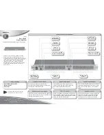
Adjustment and checking Loacation:
Note:
It is useful to use the jig for checking the waveform. (Refer to Ser-
vicing Notes on page 8)
D101
CN101
IC101
CN105
IC151
IC190
1
7
1. I+3V
2. IOP
3. GND
4. TE
5. FE
6. VC
7. RF
– BD (MD) BOARD (Component Side) –
– BD (MD) BOARD (Conductor Side) –
Содержание HCD-CP500K
Страница 7: ...7 HCD CP500K CP500MD SERVICE POSITION OF THE TAPE MECHANISM DECK Tape mechanism deck CN301 CN303 ...
Страница 39: ...39 HCD CP500K CP500MD MEMO ...
Страница 47: ...HCD CP500K CP500MD 47 47 7 4 SCHEMATIC DIAGRAM CD BOARD Page 52 ...
Страница 49: ...HCD CP500K CP500MD 49 49 7 6 SCHEMATIC DIAGRAM BD BOARD 1 2 Page 50 Page 50 Page 50 ...
Страница 50: ...HCD CP500K CP500MD 50 50 7 7 SCHEMATIC DIAGRAM BD BOARD 2 2 Page 49 Page 49 Page 49 Page 57 Page 57 ...
Страница 55: ...HCD CP500K CP500MD 55 55 7 12 SCHEMATIC DIAGRAM TC BOARD IC B D Page 52 ...
Страница 57: ...HCD CP500K CP500MD 57 57 7 14 SCHEMATIC DIAGRAM DIGITAL BOARD IC B D IC B D IC B D Page 50 Page 50 Page 52 ...
Страница 59: ...HCD CP500K CP500MD 59 59 7 16 SCHEMATIC DIAGRAM CONTROL SECTION Page 53 Page 52 Page 52 ...
Страница 93: ...93 HCD CP500K CP500MD MEMO ...