


7-1
SECTION 7
ELECTRICAL ADJUSTMENT
DVP-S7700
7-1. Power Supply Check
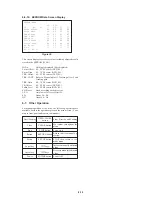
1. HS-930SH Board
Mode
E-E
Instrument
Digital voltmeter
+5.2V Check
Test point
CN201
1
pin
Specification
5.2 V ± 0.2 V
+3.3V Check
Test point
CN201
4
pin
Specification
3.3 V ± 0.2 V
EVER+5V Check
Test point
CN201
6
pin
Specification
5.4 V ± 0.2 V
P_CONT Check
Test point
CN201
8
pin
Specification
4 V – 5 V
AU +12V Check
Test point
CN201
9
pin
Specification
12 V V
AU –12V Check
Test point
CN201
!¡
pin
Specification
–12 V V
–12V Check
Test point
CN201
!™
pin
Specification
–12 V V
MTR +12V Check
Test point
CN201
!¢
pin
Specification
12 V V
Checking method:
1) Confirm that each voltage satisfies the specification.
In making adjustment, refer to 7-4. Adjustment
Related Parts Arrangement.
Note:
During diagnostic check, the characters and color bars can
be seen only with the NTSC monitor. Therefore, for diag-
nostic check, use the monitor that supports both NTSC
and PAL modes.
Use the reference disc for PAL for check, and use the ref-
erence disc for NTSC for adjustment.
This section describes procedures and instructions necessary for
adjusting electrical circuits in this set.
Instruments required:
1) Color monitor TV
2) Oscilloscope 1 or 2 phenomena, band width over 100 MHz,
with delay mode
3) Frequency counter (over 8 digits)
4) Digital voltmeter
5) Standard commander (RMT-D107E/D107P)
6) DVD reference disc
HLX-501 (J-6090-071-A) (dual layer) (NTSC)
HLX-503 (J-6090-069-A) (single layer) (NTSC)
HLX-507 (J-6090-078-A)(dual layer) (PAL)
HLX-506 (J-6090-077-A) (single layer) (PAL)
7) Extension cable (J-6090-079-A)
MB-84 (CN601)
↔
FL-107 (CN153)
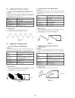
+1.0
–2.0
+2.0
–1.0
+2.0
–1.0
+1.0
–2.0
Содержание DVP-S7700
Страница 11: ...1 1 SECTION 1 GENERAL DVP S7700 This section is extracted from AEP UK model instruction manual 3 864 941 31 ...
Страница 12: ...1 2 ...
Страница 13: ...1 3 ...
Страница 14: ...1 4 ...
Страница 15: ...1 5 ...
Страница 16: ...1 6 ...
Страница 17: ...1 7 ...
Страница 18: ...1 8 ...
Страница 19: ...1 9 ...
Страница 20: ...1 10 ...
Страница 21: ...1 11 1 11 E ...
Страница 36: ...DVP S7700 4 3 4 4 4 1 FRAME SCHEMATIC DIAGRAM 1 2 FRAME 1 2 ...
Страница 37: ...DVP S7700 4 5 4 6 FRAME SCHEMATIC DIAGRAM 2 2 FRAME 2 2 ...
Страница 39: ...DVP S7700 4 9 RF SERVO TK 47 DVP S7700 1 669 298 05 13 13 TK 47 BOARD SIDE B A B C D E F G H 1 2 3 4 5 6 ...
Страница 41: ...DVP S7700 4 13 4 14 TK 47 RF SERVO 2 SCHEMATIC DIAGRAM Ref No TK 47 board 3 000 series RF SERVO 2 TK 47 2 2 ...
Страница 71: ...DVP S7700 4 73 4 74 FP 75 FL DRIVER SCHEMATIC DIAGRAM Ref No FP 75 board 1 000 series FL DRIVER FP 75 ...