background image

16

- Output regulation (pins 1, 2, 8): IC7514 stabilizes output voltage by controlling T-on and so the frequency and the duty
cycle.

Start pulse to T7525 is determined by pin 8 circuit (see fig 7.5).
Then a sawtooth voltage V2 is generated at pin 2. Stop pulse to T7525 is produced when V2 reaches Vcont.
Output control is done by the following way:

If output is higher, V1 is higher, Vcont is lower, T-on and output will be reduced.
If output is lower, output will be increased.
Output voltage of supply can be adjusted by R3518.

Mains voltage variation is stabilized in the following way:

If mains voltage is higher, slope in the sawtooth voltage V2 is higher, stop point is reached before and T-on is
reduced.
If mains voltage is lower, T-on is increased.

7.5.3   Protections

- Overload protection (pin 2): This is produced if T-on is increased till V2 voltage reaches the foldback point (see fig 7.5).
The IC will switch into overload mode (off and on continuously).
- Output voltage protections (pin 6): Limiting values of V6 voltage (7.25V and 16V) provide under and overvoltage protections
for the circuit.
- Mains overvoltage (pin 3): The voltage at pin 3 IC7515 is a measure for the mains voltage and so the DC voltage across
C2505.  As soon as the voltage V3 reaches 6.6V, the supply will stop running.

7.5.4   Secondary side

- Line supply:

Line supply present at capacitor C2530 should be adjusted to the correct value (depending on the

TRC) by means of P3518. This supply is also used to 33V varicap voltage by D6602 (see diagram E).
- Sound supply (+11V): This supply is used for sound output amplifier and to feed following stabilizers.
- +8V stabilizer: A reference voltage obtained by a resistor divider R3503 and R3505 is amplified in T7501 and T7502
transistors till diode D6572 conducts stabi8V output. When the set switch to stand by, standby voltage is 0V,
then T7501 is cut, and +8V is reduced to 0V.
- +5V stabilizer: +5V for small signal is made by and D6573 T7577  circuit. R3577 is connected to +8V to switch off +5V
when the set is in stand by mode.
- +5V stand by: +5STB is regulated by T7575 and D6570. A positive power on reset signal (POR) is obtained in the
collector of T7571, which one is cut during start up till R3576 has 0.6V.

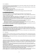
Figure 7.5 Power supply signals

Содержание CTS-AA

Страница 1: ...CHASSIS CTS AA SERVICE MANUAL SERVICE MANUAL ...

Страница 2: ... 5 Print board layout 6 6 Electric Scheme 7 11 7 Circuit description 12 7 1 Small signal processing 12 7 2 RGB ampliers 14 7 3 Deflection 14 7 4 Sound amplifier 15 7 5 Power supply 15 7 6 Microcontroller Text 17 8 Electrical adjustments 18 9 Safety instructions 21 10 List of abbreviations 22 11 Service components 23 ...

Страница 3: ...creen display OSD menu 1 LED RED Dark in ON bright in stand by blinking with RC VCR programs 0 to 99 Tuning and operating system VST UV1315A IEC VST VHFa 48 168 MHz VHFb 175 447 MHz UHF 455 855 MHz U1343A IEC VST UHF 471 855 MHz Local operating functions Vol Prog contrast colour and brightness 2 Connection facilities Euroconector 1 Audio R 0V5 RMS 1K 17 CVBS 2 Audio R 0V2 2V RMS 10K 18 CVBS 3 Audi...

Страница 4: ... on the copper side of the main carrier Position A can be reached by first removing the mains cord from it s fixation then loosen the carrier lips 1 and then pulling the carrier panel 2 for approximately 10cm Position B can be reached from position A after disconnecting the degaussing cable Put the carrier on the line transformer side 3 Mechanical instructions ...

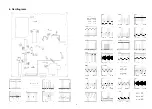
Страница 5: ...4 Oscillograms 5 ...

Страница 6: ...5 PRINT BOARD LAYOUT 6 ...

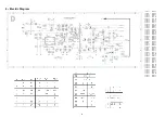
Страница 7: ...M7 9561 A2 9656 E3 6 Electric Diagram 1015 D6 1032 G8 1033 F8 1137 B7 1272 H3 2010 D7 2011 D7 2013 D8 2014 D8 2015 H6 2016 H6 2017 E9 2018 E7 2024 C6 2025 D6 2026 C6 2027 C6 2028 E6 2029 E6 2034 I7 2060 F7 2061 F6 2064 F3 2065 F3 2067 C3 2068 C3 2115 B6 2117 B9 2180 B3 2185 B3 2240 K7 2242 J2 2243 J2 2244 J2 2245 M2 2250 J6 2261 H3 2262 H2 2270 I3 2289 F3 2291 L7 2292 L7 2293 K7 2294 J7 2350 D3 23...

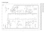
Страница 8: ...403 H7 3404 I7 3405 I7 3406 H6 3407 H5 3408 I6 3409 I6 3410 H6 3411 I7 3412 I7 3413 I5 3414 I5 3416 I4 3417 I4 3418 H5 3430 G4 3431 H4 3432 G4 3433 G3 3434 H3 3440 M7 3442 M6 3444 L7 3445 L5 3449 M3 3451 L6 3455 K7 3456 K6 3457 J5 3460 K3 3461 K4 3462 K3 3463 H2 3470 K4 3480 L6 5201 D4 5202 D4 5440 M7 5441 L6 5445 L4 5447 J4 5449 M3 5480 L6 6201 A5 6218 C5 6225 F6 6227 D5 6243 F5 6401 H5 6447 L4 6...

Страница 9: ...007 D8 3008 D8 3026 D8 3186 K5 3187 L6 3190 G8 3191 H7 3193 I6 3194 I5 3197 I6 3808 F3 3809 E4 3810 E2 3841 E5 3843 D5 3845 C5 3850 F2 3851 E3 3852 E2 3853 D3 3854 E2 3855 C3 3856 F2 3858 C3 3860 E4 3865 B2 3875 B4 3876 C4 3877 B4 3879 D2 3880 E2 3881 D1 3883 E1 3891 C2 3893 G3 5061 B7 6848 C2 6849 B2 6851 E4 6852 E4 6853 D4 6854 D4 6855 D4 6856 D4 6857 D5 7187 J4 7187 K6 7875 B5 7876 D2 9102 L6 9...

Страница 10: ...9 C4 3510 D4 3512 F4 3516 G2 3517 F4 3518 E4 3519 D3 3520 D2 3521 G3 3522 G3 3523 F3 3524 C2 3525 C3 3527 G4 3528 G4 3570 J3 3571 K3 3573 K3 3574 I3 3575 J5 3576 J3 3577 I3 5500 D2 5525 H3 5531 J2 5532 H4 5534 H2 5540 K4 5552 G2 6502 F2 6503 F2 6504 F2 6505 F2 6515 F4 6516 G2 6521 F3 6530 I2 6540 H4 6541 H2 6570 J3 6571 J3 6572 J4 6573 I3 6574 K4 7501 J5 7502 J4 7514 E3 7525 G3 7571 J3 7575 J2 757...

Страница 11: ...21 D7 3636 L7 3637 K7 3643 K3 3644 J3 3645 J3 3646 J3 3647 K3 3648 L7 3649 J3 3650 J4 3651 J4 3652 I3 3653 K4 3656 E3 3657 E3 3658 E3 3659 E3 3660 F2 3661 I7 3662 F3 3663 J7 3664 J8 3665 G8 3666 J7 3667 G8 3668 I2 3669 I2 3670 I3 3673 I8 3674 J8 3675 K8 3676 F3 3681 I7 3684 D3 3685 D3 3687 K3 3691 B2 3692 B2 3696 J8 6149 E3 6602 C7 6663 J7 6691 C2 7600 H5 7605 C7 7657 E2 7659 E2 7670 I3 7673 I8 76...

Страница 12: ...STV2248 STV2246 Figure 7 1 TV Processor block diagram ...

Страница 13: ...sitive LL modulation Sound IF is processed in SIF circuit QSS system SIF input pins 1 2 Sound is filtered from IF signal in a SAW filter K9650 1137 The IF input is present at pin 1 of 1137 and pin 2 is used as a switching input If Vpin2 0V a 40 40MHz sound carrier is filtered for L system L L signal is high T7127 conducts If Vpin2 Vpin1 a 33 40MHz sound carrier is filtered for L I BG systems L L s...

Страница 14: ...ch signals for full screen by a DC voltage or for a part of the screen by a pulse voltage Matrix After switching YUV signals are converted to RGB in the internal MATRIX circuit Saturation control is received from the µC by I2C bus APR pin 24 The APR circuit Automatic RGB Peak Regulation compensates the spread of contrast between sources If one of RGB signals exceeds the APR threshold 2440 is charg...

Страница 15: ...m B to pin 4 of IC7400 to control vertical amplitude It can be adjusted by I2C from 1 5V max vert amplitude to 6V min vert amplitude 7 2 RGB AMPLIFIERS diagram B RGB inputs The inputs of RGB amplifiers come from pins 32 31 and 30 of IC7015 Diagram A White D is adjusted in IC7015 changing the AC level of the inputs by I2C bus and cut off changing the DC level RGB amplifiers 7205 7210 7213 RGB circu...

Страница 16: ... behaviour The switching period is divided in on time when energy is extracted from the mains into the primary winding 8 12 of 5525 off time when energy in the transformer is supplied to the loads via secondary windings of 5525 and dead time when no energy is extracted or supplied Standby mode Output voltages are present when the set is on stand by due to standby is done cutting line deflection On...

Страница 17: ...nd 16V provide under and overvoltage protections for the circuit Mains overvoltage pin 3 The voltage at pin 3 IC7515 is a measure for the mains voltage and so the DC voltage across C2505 As soon as the voltage V3 reaches 6 6V the supply will stop running 7 5 4 Secondary side Line supply Line supply present at capacitor C2530 should be adjusted to the correct value depending on the TRC by means of ...

Страница 18: ...ound filter see 5 1 5 L L output is high for L system LED pin 19 The LED D6663 lights up with a low current when the television set is ON and with a high current when the set is on Standby While the set is receiving a remote control signal the led is blinking Signal I2C bus pins 20 21 This is a communication bus between the µc and the signal IC 7015 Picture and sound controls User controls brightn...

Страница 19: ...rent items can be displayed see table 8 1 Table 8 1 Service menu Settings are hexadecimal values Pre setting values When E2PROM is replaced pre setting values indicated on table 8 1 are stored by the µC see 8 7 E2PROM Adjust by Service Mode When a item is selected using V V keys of remote control it can be adjusted Items 5 16 and 17 have fixed values pre setting values rest of items see 8 2 to 8 7...

Страница 20: ...d in 8 3 1 Adjust the value of AFC coarse item 1 of Service menu to 00 and the item value of AFC fine item of Service menu to 40 Increase the AFC coarse value just till adjusting symbol is or and adjust AFC Fine to fine a value just in the middle of the range fulfilling the correct symbol Multistandard sets TV should be tuned in the first half of BI L channel Repeat the AFC Manual AFC adjustment p...

Страница 21: ...er the screen by service menu item 19 Vertical centring Occasionally it is possible to correct the vertical centring cutting resistors R3400 or R3401 TXT Shift Horizontal shift of OSD or TXT can be adjusted by item 20 of service menu 8 7 Options The type of chassis is defined by items 21 and 22 of service menu The following alternatives are available Important note All the chassis have identificat...

Страница 22: ...uld be caried out The power supply and deflection circuitry on the chassis the CRT panel and the neck of the CRT should be cleaned 9 Safety instructions maintenance instructions warning and notes Warnings 1 In order to prevent damage to IC s and transistors any flash over of the EHT should be avoided To prevent damage to the picture tube the method indicated in Fig 9 has to be applied to discharge...

Страница 23: ... Line Output Transformer MUTE PROG 0 Only for sets whithout SCART AV low for program 0 muting the sound high for program 1 39 NIL Non InterLace NTSC National Television System Committee OSD On Screen Display OSD FAST BLANKING Fast blanking info from OSD generator in µC to video controller IC7015 6D for blanking the RGB info to enable OSD G insertion OSD G Green info from OSD generator in µC to vid...

Страница 24: ...23 11 2 Electromechanical CTS AA CHASIS 11 REPLACEMENT PARTS LIST CTS AA CHASIS 11 1 Electrical TABLE11 ...

Страница 25: ... GREY MA IVORY GO DARK GREY VE GREEN RS PINK RJ RED AZ BLUE PL SILVER HOW TO ORDER EXAMPLE FRONT CABINET OF TV700TX COLOUR BLUE A 14 TV700TX AZ TV MODEL SCREEN POSITION COLOUR 11 3 Mechanical chasis and switches CTS AA CHASIS ...

Отзывы: