TM150
OTHERS
6 – 11
CONFIDENTIAL
DRAFT
■
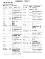
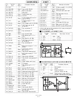
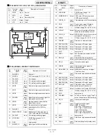
IC702 VHITK11131C-1R (TK11131C): REGULATOR
■
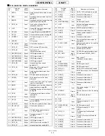
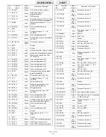
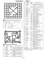
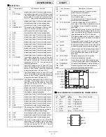
IC704 (LR38863): DISPLAY CONTROLLER
Pin
No.
Terminal
name
Input/
Output
Description of terminal
1
CONT
Input
Control
2
GND
-
Ground
3
NP
Input
Capacitor (Vref)
4
VOUT
Output
Output
5
VIN
Input
Input
Pin
No.
Terminal
name
Input/
Output
Description of terminal
1
DUMMY4
-
Dummy 4
2
VDDPLL
-
PLL Power supply 1.8 V (1.6 V~ 2.0 V)
3
PLLGND
-
PLL Ground
4
PLLDIV0
Input
PLL multiply switching signal
5
PLLDIV1
Input
PLL multiply switching signal
6
HSD0
Input/
Output
Data bus for high-speed serial transfer
7
HSD1
Input/
Output
Data bus for high-speed serial transfer
8
HSD2
Input/
Output
Data bus for high-speed serial transfer
9
HSWRD
Input/
Output
Read/Write determination signal for
high-speed serial transfer
10
HSEN
Input/
Output
High-speed serial data effective
signal High is active
11
HSCK
Input/
Output
Standard clock for high-speed
serial transfer (5 to 33 MHz)
12
DUMMY3
-
Dummy 3
13
PWM1/PORT8
Output PWM output 1 General-purpose
PORT output (default) (Not used)
14
PLLDIV2
Input
PLL multiply switching signal
15
VDDCORE
-
CORE Power supply 1.8 V
(1.6 V~ 2.0 V)
16
GND
-
Logic ground
17
SUBWR_B
Input/
Output
Light signal for External display
1
CONT
500K
320K
VIN
VOUT
Bandgap
Reference
Control
Circuit
Over Heat &
Over Current
Protection
2
GND
3
NP
5
4
- +
18
GND
-
Logic ground
19
VDDCORE
-
CORE Power supply 1.8 V
(1.6 V~ 2.0 V)
20
PWM0/PORT3
Output PWM output 0 General-purpose
PORT output (default)
21
SUBCS_B
Input/
Output
Chip select signal for External display
22
CS_B
Input/
Output
Device select signal (Display is
active when CS_B is "Low")
23
VDDIO
-
IO Power supply 3.0 V (2.7 V~ 3.3 V)
24
LCDINT
Output External interrupt signal (Starting
varies when interruption occurs.)
25
GTDIO_B
Output MPEG4ASIC internal core power-
cut signal ("Low" is active.)
26
VDDIO
-
IO Power supply 3.0 V (2.7 V~ 3.3 V)
27
SUBDB1
Input/
Output
Data bus for External display
28
BDATA[5] (B5)
Output Display panel B output signa
29
BDATA[5] (B4)
Output Display panel B output signa
30
BDATA[5] (B3)
Output Display panel B output signa
31
GND
-
Logic ground
32
TESTI
Input
Test terminal (Connected to GND
normally)
33
BSHS_B
Input/
Output
External Bit Stream horizontal
synchronization signal ("Low" is active)
34
WR_B
Input/
Output
Host write strobe signal
35
SUBRS
Input/
Output
Data determination signal for
External display
36
MP4 RESET_B
Output MPEG4ASIC reset control signal
("Low" is active)
37
HSD6
Input/
Output
Data bus for high-speed serial transfer
38
BDATA[2] (B2)
Output Display panel B output signal
39
BDATA[2] (B1)
Output Display panel B output signal
40
BDATA[2] (B0)
Output Display panel B output signal
41
EXCS_B1
Input/
Output
Chip select output 1 (internal
decode output) (Not used)
42
XOUT
Output Oscillation circuit output (Not used)
43
VDDIO
-
IO Power supply 3.0 V (2.7 V~ 3.3 V)
44
GND
-
Logic ground
45
SCANEN
Input
Full scan effective signal "High" is
active (Connected to GND normally)
46
RD_B
Input/
Output
Host read strobe signal
47
RSP
Input/
Output
Register selection signal
HOST_IF section :
RSP =Low...Display access
RSP = High...Control access
Hyper_Serial section :
RSP = Low...Control acces
RSP = High...Display access
48
GND
-
Logic ground
49
HSD3
Input/
Output
Data bus for high-speed serial transfer
50
DCLK
Input/
Output
Data sampling clock (display clock)
Pin
No.
Terminal
name
Input/
Output
Description of terminal
*
*
Содержание TM150
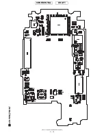
Страница 61: ...TM150 CIRCUIT DIAGRAM AND PWB LAYOUT 5 13 CONFIDENTIAL DRAFT MAIN PWB_FRONT ...
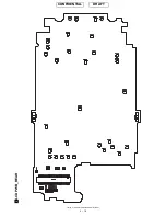
Страница 62: ...TM150 CIRCUIT DIAGRAM AND PWB LAYOUT 5 14 CONFIDENTIAL DRAFT MAIN PWB_REAR ...
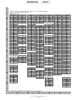
Страница 63: ...TM150 CIRCUIT DIAGRAM AND PWB LAYOUT 5 15 CONFIDENTIAL DRAFT LCD PWB_FRONT ...
Страница 64: ...TM150 CIRCUIT DIAGRAM AND PWB LAYOUT 5 16 CONFIDENTIAL DRAFT LCD PWB_REAR ...

