TM150
OTHERS
6 – 17
CONFIDENTIAL
DRAFT
■
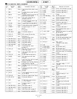
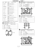
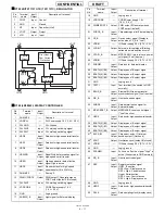
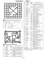
IC802 RF3146
■
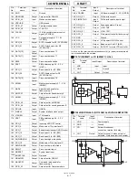
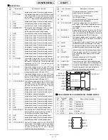
IC804 VHIR5322N29-1L(R5322N002B): POWER SUPPLY
Pin
No.
Teminal name
Description of terminal
1
NC
Internal circuit node. Do not externally connect.
2
VCC2 GSM
Contorolled voltage input to the GSM driver stage.
This voltage is part of the power control function
for the module. This node must be connected to
VCC OUT. This pin should be externally decoupled.
3
NC
Internal circuit node. Do not externally connect.
4
GND
Internally connected to the package base.
5
GND
Internally connected to the package base.
6
GSM900 OUT
RF output for the GSM bands. This is a 50
Ω
output. The output matching circuit and
DC-block are internal to the package.
7
GND
Internally connected to the package base.
8
NC
Internal circuit node. Do not externally connect.
9
NC
Internal circuit node. Do not externally connect.
10
NC
Internal circuit node. Do not externally connect.
11
NC
Internal circuit node. Do not externally connect.
12
NC
Internal circuit node. Do not externally connect.
13
NC
No internal or external connection.
14
NC
Internal circuit node. Do not externally connect.
15
NC
Internal circuit node. Do not externally connect.
16
NC
Internal circuit node. Do not externally connect.
17
NC
Internal circuit node. Do not externally connect.
18
VCC3 GSM
Controlled voltage input to the GSM output
stage. This voltage is part of the power control
function for the module. This node must be
connected to VCC OUT. This pin should be
externally decoupled.
19
VCC OUT
Controlled voltage output to feed VCC2 and
VCC3. This voltage is part of the power control
function for the module. It cannot be connected
to any pins other than VCC2 and VCC3.
20
VCC OUT
Controlled voltage output to feed VCC2 and
VCC3. This voltage is part of the power control
function for the module. It cannot be connected
to any pins other than VCC2 and VCC3.
21
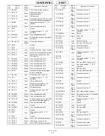
VCC3 DCS/PCS Controlled voltage input to the DCS/PCS out-
put stage. This voltage is part of the power
control function for the module. This node
must be connected to VCC OUT. This pin
should be externally decoupled.
22
NC
Internal circuit node. Do not externally connect.
23
NC
Internal circuit node. Do not externally connect.
24
NC
No internal or external connection.
25
NC
Internal circuit node. Do not externally connect.
26
NC
Internal circuit node. Do not externally connect.
27
NC
Internal circuit node. Do not externally connect.
28
NC
Internal circuit node. Do not externally connect.
29
NC
Internal circuit node. Do not externally connect.
30
GND
Internally connected to the package base.
31
DCS/PCS OUT
RF output for the DCS/PCS bands. This is a
50
Ω
output.The output matching circuit and
DC-block are internal to the package.
32
GND
Internally connected to the package base.
33
NC
Internal circuit node. Do not externally connect.
34
GND
Internally connected to the package base.
35
VCC2 DCS/PCS Controlled voltage input to the DCS/PCS
driver stage. This voltage is part of the power
control function for the module. This node
must be connected to VCC OUT. This pin
should be externally decoupled.
36
NC
No internal connection. Connect to ground
plane close to the package pin.
37
DCS/PCS IN
RF input for the DCS/PCS band.
This is a 50
Ω
output.
38
NC
No internal connection. Connect to ground
plane close to the package pin.
39
VCC1 DCS/PCS Controlled voltage input to the DCS/PCS
driver stage. This voltage is applied internal to
the package. This pin should be externally
decoupled.
40
BAND SEL
Allows external control to select the GSM or
DSC/PCS bands with a logic high or low. A
logic low enables the GSM bands, whereas a
logic high enables the DCS/PCS bands.
41
TX ENABLE
This signal enables the PA module for opera-
tion with a logic high. Both bands are disabled
with a logic low.
42
VBATT
Power supply for the module. This pin should be
externally decoupled and connected to the battery.
43
VBATT
Power supply for the module. This pin should be
externally decoupled and connected to the battery.
44
NC
Internal circuit node. Do not externally connect.
45
VRAMP
Ramping signal from DAC. A simple RC filter
may be required depending on the selected
baseband.
46
VCC1 GSM
Internally connected to VCC1 (pin39).
No external connection required.
47
GND1 GSM
Ground connection for the GSM preamplifier stage.
Connect to ground plane close to the package pin.
48
GSM900 IN
RF input to the GSM band. This is a 50
Ω
input.
Pkg
base
GND
Connect to groung plane with mulitiple via
holes. See revommended footprint.
Pin
No.
Terminal
name
Input/
Output
Description of terminal
1
CE1
Input
Chip Enable1
2
VDD
Input
Power supply
3
CE2
Input
Chip Enable2
4
VOUT2
Output
VCC for VRF
5
GND
-
Ground
6
VOUT1
Output
VCC for VTCXO
Pin
No.
Teminal name
Description of terminal
DCS/PCS IN
BAND SELECT
TX ENABLE
VBATT
VBATT
VRAMP
GSM IN
DCS/PCS OUT
GSM OUT
37
40
41
42
43
45
48
31
6
Fully Integrated
Power Control Circuit
1
2
3
4
6 VOUT
VOUT2
CE2
CE1
VDD
5 GND
Содержание TM150
Страница 61: ...TM150 CIRCUIT DIAGRAM AND PWB LAYOUT 5 13 CONFIDENTIAL DRAFT MAIN PWB_FRONT ...
Страница 62: ...TM150 CIRCUIT DIAGRAM AND PWB LAYOUT 5 14 CONFIDENTIAL DRAFT MAIN PWB_REAR ...
Страница 63: ...TM150 CIRCUIT DIAGRAM AND PWB LAYOUT 5 15 CONFIDENTIAL DRAFT LCD PWB_FRONT ...
Страница 64: ...TM150 CIRCUIT DIAGRAM AND PWB LAYOUT 5 16 CONFIDENTIAL DRAFT LCD PWB_REAR ...


