b) Connecting the oscillator and its adjustment
Connect a dummy network or branch-trunk network on to the output
of the ER-A6IN installed in the ER-A570, and connect the oscillator to
the dummy or branch-trunk network.
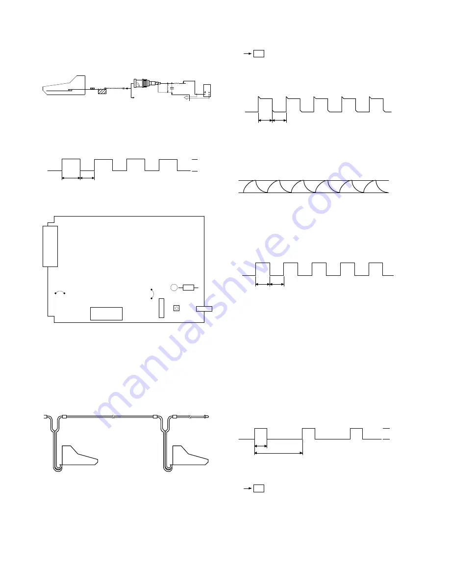
Fig. 4 Connection
∗
Waveform adjustment
Adjust VR1 until the signal waveform as shown in Fig. 5 is obtained
across TP (pin 1 of the 75115) and GND pin.
Turning VR1 clockwise extends the interval of T1.
Fig. 5 Receiver regeneration waveform (with dummy network)
Fig. 6 Board location
2
When the Branch Trunk Network and Two
ECR’S are Available.
a) Connecting terminals
Both ends of the network must be terminated with a 50
Ω
terminator. If
only two active terminals are to be tested and left on the network,
disconnect all other terminals from the network. (In this case as well,
both ends of the trunk network must be terminated with 50
Ω
).
Fig. 7 Terminal connection
b) Receive level adjustment
i)
Turn on both the objective terminal of receive level adjustment
(receiver terminal) and the terminal which sends the adjusting
signal (transmitter terminal).
ii) Run the diagnostic program JOB#603 on the transmitter terminal
to send a flag.
Key operations: MODE switch: SRV position
iii) Checking transmitter terminals’ output waveform
Using an oscilloscope, check the transmitter terminal’s output
signal waveform.
Fig. 8 Transmitter terminal’s output waveform
(at transmitter output)
At the receiver terminal, the transmitter terminal’s output
waveform is subject to attenuation and distortion due to the length
of the trunk cable (this depends on the characteristics of the cable
itself).
Fig. 9 Example of distorted signal waveform at the receiver terminal
(RG58/U 400m)
With the receiver terminal adjust VR1 (5k
Ω
) on the ER-A6IN board
until the waveform as shown in Fig. 10 is obtained at TP (pin 1 of the
75115). (For the location of VR1, see Fig. 6 Board location of this
subsection).
Clockwise rotation of VR1 extends the High level pulse width of the
signal at TP (pin 1 of the 75115).
Fig. 10 Waveform at TP (pin 1 of the 75115 IC in the receiver
terminal)
5) Other Checks (These Checks should be
done After the Receive Level Adjustment
is Completed).
1
Line driver bias control circuit
Make sure that the voltage at the
Α
-side lead of the R3 resistor
(150
Ω
, 3W) shown in Fig. 6 is properly switched.
Procedure:
i)
Connect a terminating resistor or read network to the BNC con-
nector, QCNW-6856RCZZ (Fig. 2).
ii) Run the diagnostic program JOB#604, and make sure that the
voltage at point
Α
(in Fig. 6) is switched as shown in Fig. 10.
Fig. 11 bias circuit switching waveform
Key operation:
iii) If the waveform as shown in Fig. 15 is not obtained, it is most
probable that transistor Q3 (2SA509) is defective.
2
For the other check items, refer to III. TEST FUNCTION.
C1
R1
R2
OSC
SRN connector
VOH
VOL
T1 = 580 to 620ms
T2 = 380 to 420ms
T1
T2
MC68B54
F1
VR1 IRCCN
R3
A
GND PIN
TP
CPWBX7317RC01
Parts surface
ER-A670/A650
R50
Ω
R50
Ω
ER-A670/A650
601
TL
1µ S
1µ S
3.8V
0.8V
1µ S
1µ S
12V
0V
4.3ms
17ms
602
TL
4 15
Содержание ER-A570
Страница 62: ...13 PWB layout 1 Parts side 4 19 ...
Страница 63: ...2 Solder side 4 20 ...
Страница 73: ...7 PWB layout 4 30 ...


