4
Release
The program is terminated after the above contents are printed.
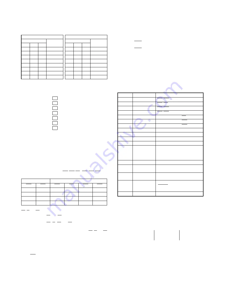
RS-232 channel setting (SW OFF: 1, SW ON: 0)
∗
Refer to the silk print on the I/F board.
ER-A5RS CN2
ER-A5RS CN1
SW1
Channel
SW1
Channel
6
5
4
3
2
1
0
0
0
Invalid
0
0
0
Invalid
0
0
1
Channel 1
0
0
1
Channel 1
0
1
0
Channel 2
0
1
0
Channel 2
0
1
1
Channel 3
0
1
1
Channel 3
1
0
0
Channel 4
1
0
0
Channel 4
1
0
1
Channel 5
1
0
1
Channel 5
1
1
0
Channel 6
1
1
0
Channel 6
1
1
1
Channel 7
1
1
1
Channel 7
2. RS-232 Channel 1 ~ 7 check
1
Activation
The program is activated by JOB#501~507.
SRV mode: 501
→
TL : Channel 1
502
→
TL : Channel 2
503
→
TL : Channel 3
504
→
TL : Channel 4
505
→
TL : Channel 5
506
→
TL : Channel 6
507
→
TL : Channel 7
2
Contents to be tested
If the channel specified by JOB#CODE is not set, the machine
performs the mis-operation processing. When the channel is set,
the machine conducts the loop check concerning the channel
specified by JOB#CODE by using the loopback connector.
The following three items are checked:
1
Control signal check
2
Data transfer check
3
Timer check (RS-232 onboard timer)
Check
1
Control signal check (ERn-DRn
•
CIn, RSn-CDn
•
CSn loop
check)
OUTPUT
INPUT
ERn
RSn
DRn
CIn
CDn
CSn
OFF
OFF
OFF
OFF
OFF
OFF
OFF
ON
OFF
OFF
ON
ON
ON
OFF
ON
ON
OFF
OFF
ON
ON
ON
ON
ON
ON
The read check about the above INPUT items and interrupt check of
CS, CI and CD are performed.
Read check:
ER and RS are switched over in the order as
shown in the above table to confirm the logic of
DR, CI, CD and CS.If the read logic is different
from the one in the table, error print-outs occur.
Interrupt check: Allows the interruption of either of CS, CI and CD
one by one. (The mask is released.)
The interruption does not take place when each
signal is turned on. Or if the interruption occurs
when a signal is turned off, error print-outs occur.
Each of the above checks should be made in four cycles.
Note) ERn control selector jumper switch on the I/F board must be
switched to the software control side.
Check
2
Data transfer check (SDn-RDn loop check)
In this check, transfer 256-byte loopback data of $00 ~
$FF.
Note) The above check should be made with the baud rate set at
9600BPS.
Check
3
Timer check
Before making check
2
, set the corresponding timer at
10ms for RCVDT activation, and check to see that:
1) TRQ1 is not generated during the execution of check
2
.
2) TRQ1 is generated in 10msec. after check
2
is fin-
ished.
3
Contents to be checked
If an error occurs during the above checks, following error print-
outs occur. Even if an error occurs during check
1
, the test is
continued after the corresponding error print-out has occurred, but
if an error occurs during the execution of check
2
or
3
, the test
is terminated after the corresponding error print-out has occurred.
Note that when check
1
,
2
or
3
terminates, the termination
print-out occurs irrespective of any errors that have occurred dur-
ing the check. (The program terminates normally only when no
error print-out has occurred.)
ERROR
ERROR PRINT
Contents
1
E1-ER DR
ERn-DRn ERR
2
E2-ER CI
ERn-CIn ERR
3
E3-RS CD
RSn-CDn ERR
4
E4-RS CS
RSn-CSn ERR
5
E5-CI INT
Interruption error of CIn
6
E6-CD INT
Interruption error of CDn
7
E7-CS INT
Interruption error of CSn
8
E8-TXEMP
TXEMPn error
9
E9-TXEMP I
Interruption error of TXEMPn
10
E10-TXRDY
TXRDYn error
11
E11-TXRDY I
Interruption error of TXRDYn
12
E12-RCVRDY
RCVRDYn error
(Reception is impossible. TRQ1 has
occurred during execution of check
2
.)
13
E13-RCVRDY I
Interruption error of RCVRDY
14
E14-SD RD
SDn-RDn ERR
(Data error)
15
E15-SD RD
SDn-RDn ERR
(Data error, Flaming error)
16
E16-TIMER
TIMERn error
(TMRQn cannot be set after
termination of check
2
.)
17
E17-TIMER I
Interruption error of TRQ1
Errors that may occur during check
1
(control signal check): E1 ~ E7
Errors that may occur during check
2
(data transfer check): E8 ~
E15
Errors that may occur during check
3
(timer check): E12, E16 and
E17
4
Cancellation
The program automatically terminates when a check is finished.
Termination print-out:
50n
n : 1 ~ 7
3 2
Содержание ER-A570
Страница 62: ...13 PWB layout 1 Parts side 4 19 ...
Страница 63: ...2 Solder side 4 20 ...
Страница 73: ...7 PWB layout 4 30 ...


