background image

9

9-1

9-2

25WF30

No.

Adjustment point

Adjustment Condition / Procedure

W

aveform or others

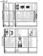
1

CONVER-

GENCE

ADJUSTMENT

(T

o be done

after the purity

adjustment.)

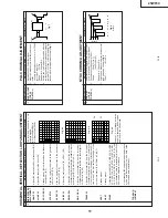
1.

Receive the Crosshatch Pattern signal.

2

.

Using the remote controller

, call NORMAL

mode.

Static convergence

1.

T

urn the 4 - pole magnet to a proper opening

angle in order to superpose the blue and red

colours.

2.

T

urn the 6 - pole magnet to a proper opening

angle in order to superpose the green colour

over the blue and red colours.

Dynamic convergence

1.

Adjust the convergence on the fringes of the

screen in the following steps.

a)

Fig. 5-1:

Drive the wedge at point "a" and swing the

deflection coil upward.

b)

Fig. 5-2:

Drive the wedge at point "b" and "c" and

swing the deflection coil downward.

c)

Fig. 5-3:

Drive the "c" wedge deeper and swing the

deflection coil rightward.

d)

Fig. 5-4:

Drive the "b" wedge deeper and swing the

deflection coil leftward.

2.

Fix all the wedges on the CR

T

 and apply glass

tape over them.

3

.

Apply lacquer to the deflection yoke lock screw

,

magnet unit (purity

, 4 - pole, 6 - pole magnets)

and magnet unit lock screw

.

Finally received the Red - only and Blue - only

signals to make sure there is no other colours

on the screen.

CONVERGENT ADJUSTMENT

Fig.

 5-1

Fig.

 5-2

Fig.

 5-3

Fig.

 5-4

Fig.

 5-5

Fig.

 5-6

 R  G  B

 R

 G

 B

 CR

T

 Neck

 Lacquer

 Purity Magnet

 4-Pole Magnet

 6-Pole Magnet.

26

±

 0.5mm

 B

 G

 R

B  G  R

 R  G  B

 B

 G

 R

 B  G  R

 R

 G

 B

 W

edge "a"

 W

edge "b"

 W

edge "c"

 About

100 Deg.

 About

100 Deg.

 Lacquer

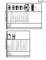
UNIFORMITY

 ADJUSTMENT

No.

Adjustment point

Adjustment Condition / Procedure

W

aveform or others

Before adjustment begin,

Horizontal magnetic field =

V

ertical magnetic field = 0.1G

Make sure degauss it.

(North direction Red uniformity)

1

.

Horizontal mf = Set to monocolour screen Red

and adjust to + 0.25G.

2.

Pay attention to the edge of CR

T

, if the land-

ing is poor

, adjust by attaching the compen-

sation magnet at the back of the CR

T

. (Refer

to figure.)

(South direction Red uniformity)

1

.

Horizontal mf = Set to monocolour screen Red

and adjust to - 0.25G.

2.

Pay attention to the edge of CR

T

, if the land-

ing is poor

, adjust by attaching the compen-

sation magnet at the back of the CR

T

.

(The same mothod is aplied for adjustment of

monocolour screen Blue for blue uniformity

,

and changing both the magnetic field for North

and South direction.)

*

During the pasting of compensation magnet,

use the crosshatch pattern.

Make sure there is no blur or bend lines oc-

cur

.

If the blur or bend lines are serious, adjust

the location of compensation magnet to make

it better

.

1

Uniformity

adjustment

(T

o perform

after the purity

and conver-

gence

adjustment.)

(CR

T

 surface)

(CR

T

 back)

Miss landing

Compensation magnet

Содержание 25WF30

Страница 1: ...BLE 13 CHASSIS LAYOUT 18 BLOCK DIAGRAM 19 WAVEFORMS 27 DESCRIPTION OF SCHEMATIC DIAGRAM 28 SCHEMATIC DIAGRAM Ë CRT UNIT 29 Ë MAIN UNIT 30 Ë POWER UNIT 34 Page Ë OPERATION UNIT 36 PRINTED WIRING BOARD ASSEMBLIES 37 SOLID STATE DEVICE BASE DIAGRAM 45 REPLACEMENT PARTS LIST Ë ELECTRICAL PARTS 46 Ë SUPPLIED ACCESSORIES 54 Ë MISCELLANEOUS PARTS 54 Ë PACKING PARTS 54 Ë CABINET PARTS 55 PACKING OF THE SE...

Страница 2: ...safety 3 Do not lift picture tube by the neck 4 Handle the picture tube only when wearing shatterproof goggles and after discharging the high voltage completely X RAY This receiver is designed so that any X Ray radiation is kept to an absolute minimum Since certain malfunctions or servicing may produce potentially hazardous radiation with prolonged exposure at close range the following precautions...

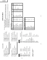
Страница 3: ...ify or not Initial data Note Once the chassis has been assembly together and ready to be POWER ON for the FIRST TIME make sure to make a short circuit JA373 and JA374 to switch to the service mode position first and then turn on the main power switch See 2 1 above Precaution If haven t done this initiation it may possibly generate excessive Beam current SERVICE MODE RASTER MODE Press the MENU butt...

Страница 4: ...in Service Mode Option While SERVICE MODE 1 on EEPROM DATA will switch to the service data Also once press the menu button at the remote controller EEPROM will switch to SERVICE MODE OPTION Once press the menu button again at the remote controller EEPROM will switch back to SERVICE MODE 1 In the service option the user data establish as below Service Mode Option No EEPROM ITEM DATA LENGTH OSD IC D...

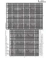
Страница 5: ...1 chip is set to 1 4 While choosing PIFVCO MODE and RF AGC set to 0 0 and PIFVCO is set to 1 2 SERVICE MODE 2 NO EEPROM ITEM DATA LENGTH OSD IC DATA SETTING INITIAL EEPROM DATA 1 WPS 0 1 WPS 1 CHIP WPS 1 2 SUB CONTRAST 0 127 S CONT 1 CHIP CONTRAST 127 3 NTSC PHASE NT 0 3 N PNT 1 CHIP NTSC PHASE 0 4 NTSC PHASE PAL SEC 0 3 N P PS 1 CHIP NTSC PHASE 0 5 NTSC PHASE DVD 0 3 N PD 1 CHIP NTSC PHASE 3 6 SU...

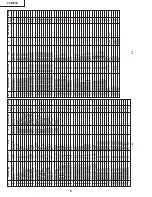
Страница 6: ... BASS 2 SP3 0 103 BASS AVM3 SP3 6 BASS 3 SP3 10 104 BASS AVM1 SP4 6 BASS 1 SP4 5 105 BASS AVM2 SP4 6 BASS 2 SP4 2 106 BASS AVM3 SP4 6 BASS 3 SP4 6 107 TREBLE AVM1 SP1 6 TRE 1 SP1 5 108 TREBLE AVM2 SP1 6 TRE 2 SP1 0 109 TREBLE AVM3 SP1 6 TRE 3 SP1 5 110 TREBLE AVM1 SP2 6 TRE 1 SP2 5 NO EEPROM ITEM DATA LENGTH OSD IC DATA SETTING INITIAL EEPROM DATA 111 TREBLE AVM2 SP2 6 TRE 2 SP2 2 112 TREBLE AVM3 ...

Страница 7: ... M 35 STTM Factory CH J8 193 25 NTSC M 36 STTM Factory CH J10 205 25 NTSC M 37 STTM Factory CH J12 217 25 NTSC M 38 STTM Factory CH J38 217 25 NTSC M SHIPPING SETTING AND CHECKING 1 The following default data has been factory set for the E 2 PROM ITEMS DATA SETTING FACTORYSET 9 R C 238 EEh S SYSTEM B G LANGUAGE THAI SELECT MODE 1 2 3 SOFT STANDARD DYNAMIC CONTRAST COLOUR BRIGHT 0 0 0 TINT 0 0 0 SH...

Страница 8: ...e setting below is automati cally set when the SUB VOL is selected in the service mode SURROUND OFF AV MODE STANDARD S NORMAL state S VOL Max Bass OFF SOUND ADJUSTMENT 1 SUB VOL BUS ADJUST MENT 1 Receive PAL Colour Bar signal Signal content 400 Hz 100 Mod 2 Connect the probel of the meter to SI con nector 3 Select the SUB VOL in the service mode 4 Adjust the SUB VOL data to make the meter indicate...

Страница 9: ...NT Fig 5 1 Fig 5 2 Fig 5 3 Fig 5 4 Fig 5 5 Fig 5 6 R G B R G B CRT Neck Lacquer Purity Magnet 4 Pole Magnet 6 Pole Magnet 26 0 5mm B G R B G R R G B B G R B G R R G B Wedge a Wedge b Wedge c About 100 Deg About 100 Deg Lacquer UNIFORMITY ADJUSTMENT No Adjustment point Adjustment Condition Procedure Waveform or others Before adjustment begin Horizontal magnetic field Vertical magnetic field 0 1G Ma...

Страница 10: ...etween TP1601 TP1602 Ammeter full scale 3mA range TP1602 is connected at the side of the am meter TP1601 is connected at the side of the am meter 4 Adjust the beam current to 1 6mA 20µA with R1759 sub contrast VR Note Apply the adjustment after aging with the beam current 1 400 50µA or more for 30 min or more On the white or green monocolor screen SUB CONT ADJUSTMENT 3 WHITE BALANCE BACK GROUND CU...

Страница 11: ...he linearity is achieved E 2 V CENT 50 Align the center of the screen to the geometric center of CRT E 5 H CENT 50 Align the center of the screen to the geometric center of CRT E 5 H SIZE 50 Adjust the overscan to 8 5 0 5 E 5 E W PAR 50 Adjust the 2nd vertical line from the left end of crosshatch pattern so that the midddle 4 blocks are straight E 2 Refer to Fig 6 1 E W COR 50 Adjust the 2nd verti...

Страница 12: ...P Option STANDARD NORMAL SET TING WARM for more REDDISH direction changing COOL for more BLUISH direction changing No Adjustment point Adjustment Condition Procedure Waveform or others FUNCTION OPERATION CHECKING 2 VIDEO AUDIO 9 HEADPHONE OUTPUT CHECKING 1 Receive the PAL Colour Bar signal with sound 400 Hz 100 modulation 50 kHz Dev 2 Maximum volume and check the headphone output with 400 kHz soun...

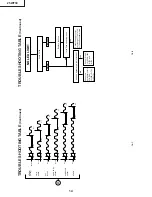
Страница 13: ... D1200 Power LED turn on and off NO RASTER Normal Check CRT connector KY H bias Is pin 10 of IC700 in L level Abnormal Check IC850 Check protecter circuit and its related parts pin 2 of IC1000 vertical pulse Check the power circuit consisting of IC700 Q700 IC750 and IC602 Yes Yes RED Yes Bus error No See many often D1200 flashes in red This indicates which IC to check up No A Does horizontal circu...

Страница 14: ...e the Fuse Is the Fuse again blown out Does 5V appear at pin 22 of IC1000 Blown out No No Yes Yes Check IC1000 IC1002 Q1002 Q752 and Q753 Check F3700 NO LED LIGHT E 2 PROM IC1001 V C D IC800 PLL Tuner S CONTROL IC300 AV SWITCH IC400 OTHER 500 500 2000 ms 2000 ms 500 500 2000 ms 500 500 2000 ms 500 500 2000 ms 500 500 2000 ms 500 500 Bus Err Bus Err Bus Err Bus Err Bus Err Bus Err A TROUBLE SHOOTIN...

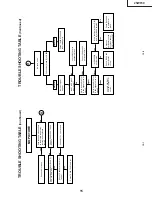
Страница 15: ...eck pins 6 and 7 of IC800 Abnormal B Noise or signal appear Is AV1 AV2 or AV3 input normal Check Q455 and its peripheral circuit Check TU200 SF200 and their related parts Yes No Which does pin 43 of IC400 appear noise or signal Which does pin 39 of IC800 appear noise or signal Check IC400 and its peripheral circuit Noise Signal Check IC400 Q401 and their peripheral circuit Is IC800 RGB out Normal ...

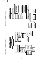
Страница 16: ...00 No No Yes Check IC300 Yes Check IC1300 and its peripheral parts Set S Volume at maximum Do pins 12 15 of IC300 work Check IC301 and its peripheral circuit No Yes Yes Yes No Turn on colour control Does colour appear NO SPECIFIC COLOUR C Is only RF signal s colour abnormal Set the colour control Turn on colour system forced switch Does colour appear Fix cotrol to coloured system Check TU200 Q455 ...

Страница 17: ...be readjusted in service mode Turn on colour system forced switch Does colour appear APG circuit Check IC800 and its peripherals Yes Yes White balance Check RGB output circuit of IC800 Check IC800 No Yes No Check D1664 and its peripherals PAL SECAM NTSC4 43 Check X800 pin 12 of IC800 and their peripherals No No Is chroma input level at pin 43 of IC800 proper Ref value 100 500mVp p Yes Fix control ...

Страница 18: ...6 5 4 3 2 1 A B C D E F G H 18 25WF30 CHASSIS LAYOUT ...

Страница 19: ...6 5 4 3 2 1 A B C D E F G H 19 25WF30 BLOCK DIAGRAM 1 ...

Страница 20: ...21 25WF30 20 25WF30 8 7 10 9 6 5 4 3 2 1 A B C D E F G H 17 16 19 18 15 14 13 12 11 BLOCK DIAGRAM 2 ...

Страница 21: ...23 25WF30 22 25WF30 8 7 10 9 6 5 4 3 2 1 A B C D E F G H 17 16 19 18 15 14 13 12 11 BLOCK DIAGRAM 3 ...

Страница 22: ...25 25WF30 24 25WF30 8 7 10 9 6 5 4 3 2 1 A B C D E F G H 17 16 19 18 15 14 13 12 11 BLOCK DIAGRAM 4 ...

Страница 23: ...6 5 4 3 2 1 A B C D E F G H 26 25WF30 BLOCK DIAGRAM 5 ...

Страница 24: ...1 7v Pin 4 Vp p 2 04v Pin 5 Vp p 58 4v Pin 6 Vp p 288v Pin 7 Vp p 1090v Pin 8 Vp p 10v Pin 9 Vp p 4 64v Pin 10 Vp p 1 0v Pin 11 Vp p 1 0v Pin 12 Vp p 4 6v Pin 13 Vp p 3 96v Pin 14 Vp p 3 88v Pin 15 Vp p 150 0v Pin 16 Vp p 150 0v Pin 17 Vp p 150 0v Pin 18 Vp p 448 0v ...

Страница 25: ...ECTED WITH AC MAINS VOLTAGE WHENSERVICINGTHEAREA CONNECTANISOLATINGTRANS FORMER BETWEEN TV RECEIVER AND AC LINE TO ELIMINATE HAZARD OF ELECTRIC SHOCK NOTES 1 The unit of resistance ohm is omitted K 1000 ohms M Meg ohm 2 All resistors are 1 16 watt unless otherwise noted 3 All capacitors are µF unless therwise noted P µµF VOLTAGE MEASUREMENT CONDITIONS 1 Voltage in parenthesis measured with no Sign...

Страница 26: ...6 5 4 3 2 1 A B C D E F G H 29 25WF30 SCHEMATIC DIAGRAM CRT Unit ...

Страница 27: ...31 25WF30 30 25WF30 8 7 10 9 6 5 4 3 2 1 A B C D E F G H 17 16 19 18 15 14 13 12 11 SCHEMATIC DIAGRAM MAIN 1 2 Unit ...

Страница 28: ...33 25WF30 32 25WF30 8 7 10 9 6 5 4 3 2 1 A B C D E F G H 17 16 19 18 15 14 13 12 11 SCHEMATIC DIAGRAM MAIN 2 2 Unit ...

Страница 29: ...35 25WF30 34 25WF30 8 7 10 9 6 5 4 3 2 1 A B C D E F G H 17 16 19 18 15 14 13 12 11 SCHEMATIC DIAGRAM POWER Unit ...

Страница 30: ...6 5 4 3 2 1 A B C D E F G H 36 25WF30 SCHEMATIC DIAGRAM OPERATION Unit ...

Страница 31: ...6 5 4 3 2 1 A B C D E F G H 37 25WF30 PWB C CRT Unit Wiring Side PRINTED WIRING BOARD ASSEMBLIES ...

Страница 32: ...39 25WF30 38 25WF30 8 7 10 9 6 5 4 3 2 1 A B C D E F G H 17 16 19 18 15 14 13 12 11 PWB A MAIN Unit Wiring Side ...

Страница 33: ...41 25WF30 40 25WF30 8 7 10 9 6 5 4 3 2 1 A B C D E F G H 17 16 19 18 15 14 13 12 11 PWB A MAIN Unit Chip Parts Side ...

Страница 34: ...43 25WF30 42 25WF30 8 7 10 9 6 5 4 3 2 1 A B C D E F G H 17 16 19 18 15 14 13 12 11 PWB B POWER Unit Wiring Side ...

Страница 35: ...6 5 4 3 2 1 A B C D E F G H 44 25WF30 PWB D OPERATION Unit Wiring Side ...

Страница 36: ...7L iX0037 KA78S09P 1 12 1 21 42 22 JC EMITTER BASE 1 4 36 25 37 24 48 13 COLLECTOR iX3422CE BH3543F MM1437BF 2SC2735 CXA2089Q 1 10 8 5 1 4 24 13 1 12 8 5 1 4 20 11 1 2 3 6 5 4 KA358P VSiMZ1A TDA9181T AN5891K MiP0253 EMITTER BASE COLLECTOR 2SC3198 Y 2SC3198 G 2SC1959 Y DX0452CE DX0336CE SE120N CATHODE ANODE 1 2 3 1 3 ANODE RED CATHODE COMMON ANODE GREEN A K COLLECTOR BASE EMITTER PX0414CE PX0274CE ...

Страница 37: ...e AB D605 RH DX0475CEZZ R Diode AB D620 RH DX0475CEZZ R Diode AB D621 RH DX0475CEZZ R Diode AB D622 RH DX0475CEZZ R Diode AB D625 RH DX0475CEZZ R Diode AB D626 RH EX0610GEZZ R Zener Diode AA D1000 RH EX0619GEZZ R Zener Diode AA D1001 RH EX0619GEZZ R Zener Diode AA D1002 RH EX0619GEZZ R Zener Diode AA D1003 RH EX0619GEZZ R Zener Diode AA D1004 RH EX0619GEZZ R Zener Diode AA D1005 RH EX0619GEZZ R Ze...

Страница 38: ...1HW224M R 0 22 50V Electrolytic AB C457 VCKYCY1CF104Z R 0 1 16V Ceramic AA C458 VCKYCY1HF103Z R 0 01 50V Ceramic AA C459 VCEA0A1CW107M R 100 16V Electrolytic AC C460 VCKYCY1HB822K R 8200p 50V Ceramic AB C461 VCKYCY1HF103Z R 0 01 50V Ceramic AA C462 VCCCCY1HH561J R 560p 50V Ceramic AB C463 VCKYCY1HF103Z R 0 01 50V Ceramic AA C468 VCKYCY1HF103Z R 0 01 50V Ceramic AA C469 VCEA0A1HW105M R 1 50V Electr...

Страница 39: ...trolytic AB C1311 VCEA0A1CW106M R 10 16V Electrolytic AB C1312 VCEA0A1CW106M R 10 16V Electrolytic AB C1313 VCEA0A1EW227M R 220 25V Electrolytic AB C1320 VCKYCY1HB102K R 1000p 50V Ceramic AA C1321 VCEA0A1CW106M R 10 16V Electrolytic AB C1322 VCKYCY1HB102K R 1000p 50V Ceramic AA C1323 VCEA0A1CW106M R 10 16V Electrolytic AB C1324 VCKYCY1HB102K R 1000p 50V Ceramic AA C1325 VCEA0A1CW106M R 10 16V Elec...

Страница 40: ... Oxide AA R425 VRS CY1JF331J R 330 1 16W Metal Oxide AA R434 VRS CY1JF101J R 100 1 16W Metal Oxide AA R435 VRS CY1JF151J R 150 1 16W Metal Oxide AA R436 VRS CY1JF101J R 100 1 16W Metal Oxide AA R437 VRS CY1JF151J R 150 1 16W Metal Oxide AA R438 VRS CY1JF101J R 100 1 16W Metal Oxide AA R439 VRS CY1JF151J R 150 1 16W Metal Oxide AA R440 VRS CY1JF101J R 100 1 16W Metal Oxide AA R441 VRS CY1JF151J R 1...

Страница 41: ... 1 16W Metal Oxide AA R5411 VRS CY1JF122J R 1 2k 1 16W Metal Oxide AA R5412 VRS CY1JF152J R 1 5k 1 16W Metal Oxide AA R5413 VRS CY1JF102J R 1k 1 16W Metal Oxide AA R5414 VRD RA2BE101J R 100 1 8W Carbon AB R629 VRS CY1JF271J R 270 1 16W Metal Oxide AA R630 VRS CY1JF271J R 270 1 16W Metal Oxide AA R631 VRS CY1JF563J R 56k 1 16W Metal Oxide AA R632 VRS CY1JF223J R 22k 1 16W Metal Oxide AA R633 VRD RA...

Страница 42: ...IT D754 RH DX0452CEZZ R Diode AH D755 RH DX0475CEZZ R Diode AB D756 RH EX0152CEZZ R Zener Diode AE D757 RH EX0643GEZZ R Zener Diode AB D758 RH DX0475CEZZ R Diode AB D759 RH DX0475CEZZ R Diode AB D760 RH DX0475CEZZ R Diode AB D761 RH DX0475CEZZ R Diode AB D1534 RH DX0279CEZZ R Diode AB D1535 RH EX0665GEZZ R Zener Diode AA D1576 RH DX0127CEZZ R Diode AC D1620 RH DX0475CEZZ R Diode AB å D1621 RH EX06...

Страница 43: ...Carbon AA R1672 VRD RA2BE472J R 4 7k 1 8W Carbon AA R1673 VRD RA2EE822J R 8 2k 1 4W Carbon AA R1674 VRD RM2HD182J R 1 8k 1 2W Carbon AA R1675 VRN VV3DBR33J R 0 33 2W Metal Film AA C754 RC KZ1040CEZZ 47p 1kV Ceramic C755 RC EZ0004PEZZ R 2200 35V Electrolytic AH C756 RC EZ1226CEZZ R 3300 16V Electrolytic AK C757 RC EZ1100CEZZ R 1000 25V Electrolytic AF C758 RC EZ0308CEZZ R 330 160V Electrolytic AF C...

Страница 44: ...AB D1506 RH DX0487CEZZ R Diode AC D1507 RH DX0487CEZZ R Diode AC D1508 RH DX0475CEZZ R Diode AB CAPACITORS C850 VCFYSB2EB823J R 0 082 250V Mylar AD C851 RC KZ018JCEZZ R 0 01 3kV Ceramic AC C852 VCEA0A1CW106M R 10 16V Electrolytic AB C853 VCFYFA1HA224J R 0 22 50V Mylar AB C854 VCEA0A1AW227M R 220 10V Electrolytic AB C855 VCEA0A2EW106M R 10 250V Electrolytic AD C856 VCEA0A1CW226M R 22 16V Electrolyt...

Страница 45: ...k 1 8W Carbon AA R1227 VRD RA2BE273J R 27k 1 8W Carbon AA R1228 VRD RA2BE101J R 100 1 8W Carbon AB R1229 VRD RA2BE223J R 22k 1 8W Carbon AA R1230 VRD RA2BE151J R 150 1 8W Carbon AA R1231 VRD RA2BE102J R 1k 1 8W Carbon AA R1232 VRD RA2BE102J R 1k 1 8W Carbon AA R1233 VRD RA2BE102J R 1k 1 8W Carbon AA R1250 VRD RA2BE101J R 100 1 8W Carbon AB RDA850 PRDAR0248PEFW R Heat Sink for Q1506 AF RDA1506 PRDA...

Страница 46: ...ESA R SHARP Badge AG 1 4 HDECQ0042KJSA LED R C Cover 1 5 HiNDP0026KJSA Indication Plate In Door 1 6 HPNLC0001KJSA Control Panel 1 7 JBTN 0048KJSA Power Button 1 8 MSPRC0002KJFW Spring Power Button 1 9 PKAi 0007PE00 R Door Latch AE 2 CCABB0058WEA0 Rear Cabinet Ass y 2 1 Not Available Rear Cabinet 2 2 HiNDP0265PEZZ R Rear AV Jack Indication AF Plate 1 1 1 1 6 1 7 1 4 1 2 1 5 1 8 1 3 1 9 2 1 2 2 2 FR...

Страница 47: ...Items Operation Manual Guarantee Card Batteries Infrared R C Unit Buffer Material Packing Case USE 22 STAPLES FIX THE PACKING CASE PACKING OF THE SET SHARP CORPORATION AV Systems Group Quality Reliability Control Center Yaita Tochigi 329 2193 Japan DSEM PSREC TQ1083 S Jan 2001 Printed in Japan NA KY ...

Отзывы: