
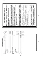


3
3-1
3-2
25WF30
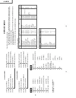
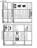
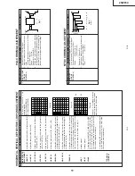
ADJUSTMENT PRECAUTIONS
This model’
s setting are adjusted in two dif
ferent ways: though the I
2
C bus control and in the
conventional analog manner
.
The adjustments via the I
2
C bus control include preset-only items
and variable data.
1.
Setting the service mode by the microprocessor
.
1
Make a short-circuit JA373 and JA374, enter into the service mode. (Adjustment through
the I2C bus control). (Use JWS Key to set as well).
2
Press the CH DOWN / UP key on the remote controller to get ready to select the mode
one by one.
3
Press the CH DOWN / UP key on the remote controller to select the modes reversibly
one by one.
4
Using the VOLUME UP/ DOWN key on the remote controller
, the data can be modified.
5
When the short circuit between JA373 and JA374 is cut of
f, it will be released from the
service mode.
2.
Factory Presetting.
1
Make a short-circuit JA373 and JA374 and turn on the main power switch. Initial values
are automatically preset, only when a new EEPROM is used (Judge with the first 4
bytes).
2
The initial data are preset as listed in page.
3
Make sure the data need modify or not (Initial data).
Note:
Once the chassis has been assembly together and ready to be POWER ON for the
FIRST TIME, make sure to make a short-circuit JA373 and JA374 to switch to the
service mode position first and then turn on the main power switch. (See 2-1 above).
Precaution: If haven’t done this initiation, it may possibly generate excessive Beam
current.
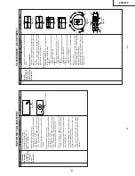
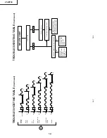
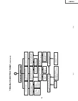
SER
VICE MODE
RASTER
MODE
Press the MENU button
at the remote controller
,
it will enter into
Service Mode Option.
Press the MENU button
again at the remote controller
,
it will jump back to
Service Mode 1.
Press service/ language for 2 sec,
it will enter into service mode 2.
Press service/ language for 2 sec again,
it will jump back to service mode 1.
FOR
W
ARD : CH DOWN KEY
REVERSE : CH UP
KEY
R-CUT
OFF
G-CUT
OFF
B-CUT
OFF
KEY
R-CUT
OFF
G-CUT
OFF
B-CUT
OFF
G-DRIVE
B-DRIVE
UP
1
KEY
2
KEY
3
KEY
7
KEY
8
KEY
DOWN
4
KEY
5
KEY
6
KEY
F/B KEY
0
KEY
3 sec.
TIME OUT
CUT
OFF
MODE
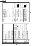
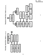
SER
VICE MODE 1
1.) In the Service Mode, Key is used to select the mode in the following order
.
CUT
OFF/ BKGD MODE
50Hz ADJ.
MODE
SER
VICE MODE 2
SUB 2
ADJ.
MODE
SER
VICE MODE
OPTION
60 Hz
ADJ.
MODE
SUB 1
ADJ.
MODE
CUT
OFF
BKGD
MODE
LA
TERAL
MODE
(R, G, B-CUT
OFF)
G-DRIVE
B-DRIVE
3 sec.
TIME OUT
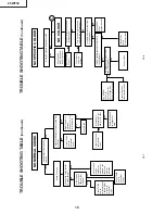
D
ATA
LENGTH
DRIVE
"—/——"
INITIAL
D
ATA
0 - 127
63
D
ATA
LENGTH
CUT
OFF
INITIAL
D
ATA
63 - 255
63
Содержание 25WF30
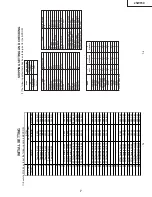
Страница 18: ...6 5 4 3 2 1 A B C D E F G H 18 25WF30 CHASSIS LAYOUT ...
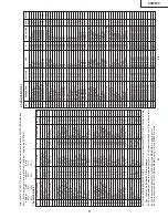
Страница 19: ...6 5 4 3 2 1 A B C D E F G H 19 25WF30 BLOCK DIAGRAM 1 ...
Страница 20: ...21 25WF30 20 25WF30 8 7 10 9 6 5 4 3 2 1 A B C D E F G H 17 16 19 18 15 14 13 12 11 BLOCK DIAGRAM 2 ...
Страница 21: ...23 25WF30 22 25WF30 8 7 10 9 6 5 4 3 2 1 A B C D E F G H 17 16 19 18 15 14 13 12 11 BLOCK DIAGRAM 3 ...
Страница 22: ...25 25WF30 24 25WF30 8 7 10 9 6 5 4 3 2 1 A B C D E F G H 17 16 19 18 15 14 13 12 11 BLOCK DIAGRAM 4 ...
Страница 23: ...6 5 4 3 2 1 A B C D E F G H 26 25WF30 BLOCK DIAGRAM 5 ...
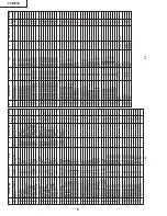
Страница 26: ...6 5 4 3 2 1 A B C D E F G H 29 25WF30 SCHEMATIC DIAGRAM CRT Unit ...
Страница 30: ...6 5 4 3 2 1 A B C D E F G H 36 25WF30 SCHEMATIC DIAGRAM OPERATION Unit ...
Страница 31: ...6 5 4 3 2 1 A B C D E F G H 37 25WF30 PWB C CRT Unit Wiring Side PRINTED WIRING BOARD ASSEMBLIES ...
Страница 35: ...6 5 4 3 2 1 A B C D E F G H 44 25WF30 PWB D OPERATION Unit Wiring Side ...


