


21S-FX10L
9 – 1
TV
21S-FX10L
Service Manual
21S-FX10L
Market
E
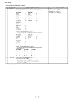
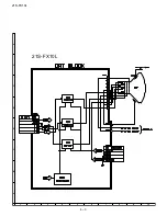
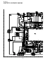
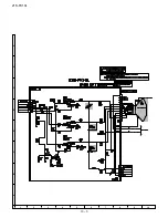
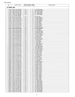
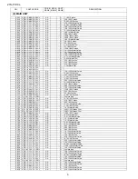
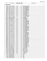
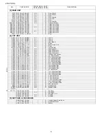
CHAPTER 9.
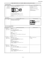
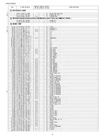
DESCRIPTION OF SCHEMATIC DIAGRAM
DESCRIPTION OF SCHEMATIC DIAGRAM
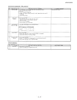
NOTES:
1. The unit of resistance "ohm" is omitted.
(K=k
Ω
=1000
Ω
, M=M
Ω
)
2. All resistors are 1/16 watt, unless otherwise noted.
3. All capacitors are
μ
F, unless otherwise noted.
(P=pF=
μμ
F)
4. (G) indicates
±
2% tolerance may be used.
5.
indicates line isolated ground.
VOLTAGE MEASUREMENT CONDITIONS:
1. All DC voltages are measured with DVM connected
between points indicated and chassis ground, line
voltage set at 120V AC and all controls set for normal
picture unless otherwise indicated.
2. All voltages measured with 1000
μ
V B & W or Color
signal.
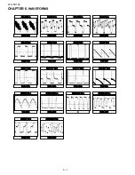
WAVEFORM MEASUREMENT CONDITIONS:
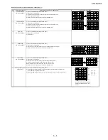
1.
Photographs taken on a standard gated color bar
signal, the tint setting adjusted for proper color. The
wave shapes at the red, green and blue cathodes of
the picture tube depend on the tint, color level and
picture control.
2.
indicates waveform check points (See chart,
waveforms are measured from point indicated to
chassis ground.)
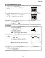
AND SHADED (
) COMPONENTS
= SAFETY RELATED PARTS.
MARK= X-RAY RELATED PARTS.
DRGANNES MARQUES
ET HACHRES (
):
PIECES RELATIVES A LA SECURITE.
MARQUE
: PIECS RELATIVE AUX RAYONS X.
This circuit diagram is a standard one, printed circuits
may be subject to change for product improvement
without prior notice.
Содержание 21SFX10L
Страница 27: ...21S FX10L 8 2 19 18 17 16 15 14 13 12 11 10 ...
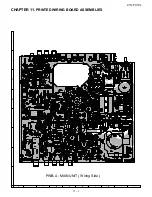
Страница 28: ...21S FX10L 8 3 A C B D E F G H 2 10 9 8 7 6 5 4 3 1 21S FX10L ...
Страница 31: ...21S FX10L 10 2 19 18 17 16 15 14 13 12 11 10 ...
Страница 32: ...21S FX10L 10 3 A C B D E F G H 2 10 9 8 7 6 5 4 3 1 ...
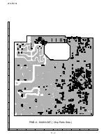
Страница 34: ...21S FX10L 11 2 PWB A MAIN UNIT Chip Parts Side A C B D E F G H 2 10 9 8 7 6 5 4 3 1 ...
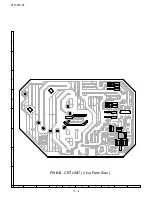
Страница 35: ...21S FX10L 11 3 PWB B CRT UNIT Wring Side A C B D E F G H 2 10 9 8 7 6 5 4 3 1 ...
Страница 36: ...21S FX10L 11 4 PWB B CRT UNIT Chip Parts Side A C B D E F G H 2 10 9 8 7 6 5 4 3 1 ...