52
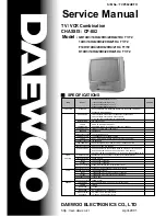
13VT-N100
13VT-N150
13VT-CN10
NO
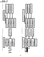
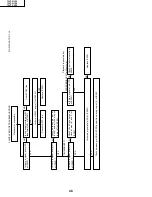
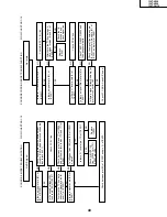
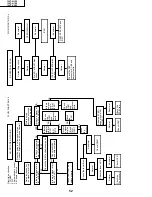
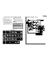
FLOW CHART NO.2-3
FLOW CHART NO.2-4
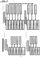
NO PICTURE, NO SOUND
YES
YES
YES
YES
YES
YES
YES
Check
the
IC401
and
adjacent
parts.
Check the IC401 and
adjacent parts.
Check the Q404
and adjacent parts.
Check the CRT
connector K1~K6 and
adjacent parts.
Pin (22) of IC401 bias
check.
IC501 (LA7830) bias
check.
D502, C509, C510 and
R511
Vertical freq check
CF631 (503kHz)
Normal
Abnormal
IC401
Abnormal
Abnormal
Normal
Normal
NO
NO
NO
NO
NO
NO
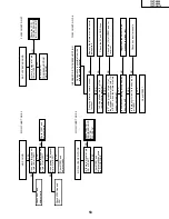
NO VERTICAL SCAN
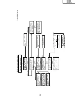
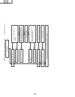
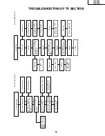
Circuit to be checked:
1. TUNER
2. PIF
3. Automatic gain control
4. 9V power source
Check the IC401 and adjacent parts
Check IC2001.
Check the tuner AGC.
Check
the
IC351.
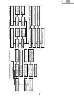
Does the noise level increase at max,
Contrast, Brightness, and Sound Control?
Is there a signal at pin
(43) of IC401?
Noise increases but
no signal is received
Is there a signal at pin
(41) of IC401?
Picture noise
decrease but sound
level varies greatly.
Check the tuner bias.
Normal
Abnormal
Abnormal
Check IC401.
Normal
Check the
Tuner circuit.
Abnormal
Check the
PC9V line.
Normal
Check IC401.
Does the 9V (+B)
appear at pin (48)
of IC401?
Is there a signal at
pin (37) of IC401?
Is there a signal at
pin (53) of IC401.
Is there a
signal at
pin (2) of
IC351
(AN
7511)?
Is there
a signal
at pins
(6) and
(8) of
IC351?
Check
the
speaker.
Check
the
IC401,
and
adjacent
parts.
Is there
a signal
at pin
(54) of
IC401?
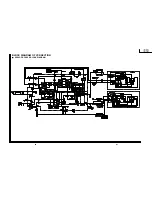
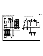
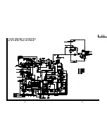
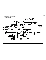
Содержание 13VT-CN10
Страница 55: ...57 13VT N100 13VT N150 13VT CN10 56 12 11 10 9 8 7 6 5 4 3 2 1 A B C D E F G H BLOCK DIAGRAM OF TV SECTION ...
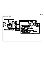
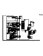
Страница 61: ...69 13VT N100 13VT N150 13VT CN10 68 12 11 10 9 8 7 6 5 4 3 2 1 A B C D E F G H OVERALL SCHEMATIC DIAGRAM ...
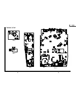
Страница 69: ...83 6 5 4 3 2 1 A B C D E F G H 13VT N100 13VT N150 13VT CN10 PWB C POWER Unit Wiring Side ...
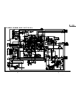
Страница 70: ...84 6 5 4 3 2 1 A B C D E F G H 13VT N100 13VT N150 13VT CN10 PWB A MAIN Unit Wiring Side ...
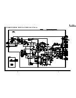
Страница 71: ...85 6 5 4 3 2 1 A B C D E F G H 13VT N100 13VT N150 13VT CN10 PWB A MAIN Unit Chip Parts Side ...

