

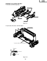


43
13VT-N100
13VT-N150
13VT-CN10
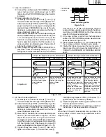
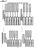
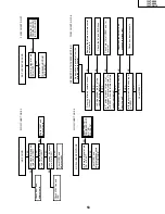
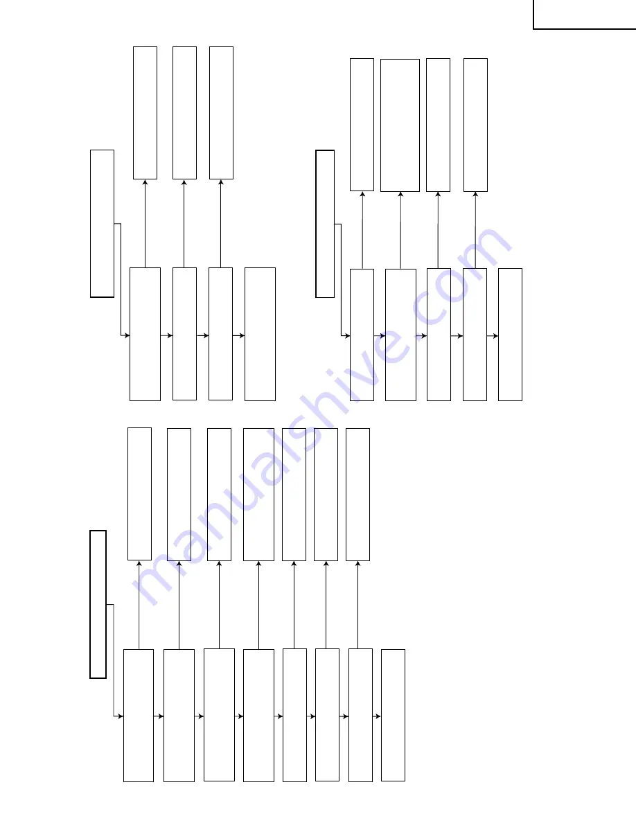
FLOW CHART NO.1-4
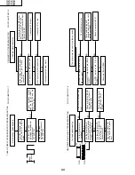
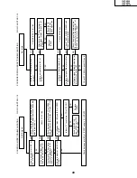
NO
NO
NO
NO
NO
NO
NO
YES
YES
YES
YES
YES
YES
YES
See FLOW CHART NO.1-6.
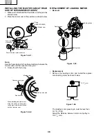
Replace the loading motor.
Check the reel disk and reel
drive unit.
Check the take up reel sensor
and all the way to IC2001.
Check between pin (6) of IC7701
and all the way up to pin (20) of
IC2001.
Check IC7701 and "L" level of
pin (5) of it.
Check between IC7701 and all
the way up to the loading motor.
LOADING MOTOR AND EJECT TROUBLESHOOTING
A cassette tape fails to eject.
Does the capstan motor start
when the EJECT button is
pressed?
Does the take-up reel disk turn
when the capstan motor is
running?
Is reel pulse at pin (80) of
IC2001 when the take-up reel
disk is turning?
Is "H" level (about 1.8V) at pin
(6) of IC7701 when reel pulse is
inputted?
Is about 11V at pin (10) of IC7701?
Is the correct voltage at the
loading motor terminal?
Does the loading motor run?
Replace the cassette cam, gear,
etc.
NO
NO
NO
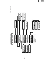
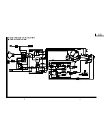
SYSTEM CONTROL TROUBLESHOOTING
FLOW CHART NO.1-5
FLOW CHART NO.1-6
No power.
YES
YES
YES
NO
NO
NO
NO
YES
YES
YES
YES
Check IC2001.
Check IC765 (PC9V GEN.)
Check IC756 and Q756
(PC5V GEN.)
Check the AT5V line.
Check pin (74) of IC2001
Check the AT8V line or the
AT12V line.
Does power control (H) signal at
pin (31) of IC2001 change from
"L" to"H" level?
Check peripheral circuit for poor
soldering of PC9V and PC5V
lines.
Check between the MC
connector and IC2001, and
between the MC connector and
pin (76) of IC2001.
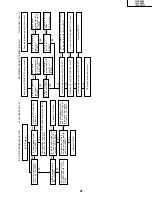
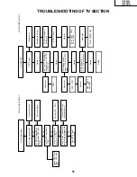
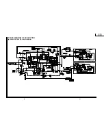
CAPSTAN MOTOR TROUBLESHOOTING
The capstan motor fails to run.
Is the voltage more than about
2.6V given to pin (4) of AC
connector?
Is the voltage at pin (3) of AC
connector 1.8~2.7V?
Is 5V at pin (8) of AC connector?
Check/replace the capstan motor.
Is the PC5V line normal?
Is the PC9V line normal?
Is 8V or 12V at pin (5) of AC
connector?
Содержание 13VT-CN10
Страница 55: ...57 13VT N100 13VT N150 13VT CN10 56 12 11 10 9 8 7 6 5 4 3 2 1 A B C D E F G H BLOCK DIAGRAM OF TV SECTION ...
Страница 61: ...69 13VT N100 13VT N150 13VT CN10 68 12 11 10 9 8 7 6 5 4 3 2 1 A B C D E F G H OVERALL SCHEMATIC DIAGRAM ...
Страница 69: ...83 6 5 4 3 2 1 A B C D E F G H 13VT N100 13VT N150 13VT CN10 PWB C POWER Unit Wiring Side ...
Страница 70: ...84 6 5 4 3 2 1 A B C D E F G H 13VT N100 13VT N150 13VT CN10 PWB A MAIN Unit Wiring Side ...
Страница 71: ...85 6 5 4 3 2 1 A B C D E F G H 13VT N100 13VT N150 13VT CN10 PWB A MAIN Unit Chip Parts Side ...


