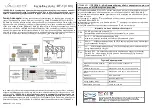
2. Name and Function of Each Part
S5U1C17W23T Manual
Seiko Epson Corporation
7
(Rev.1.1)
2.2.2
Function of Each Component
Table 2.2.2 List of the names and functions of components in each part
Component
name
Location
Function
IC
U1
S1C17W23 (16-bit MCU)
Connector header
CN1(J1)
Extension interface connector header
Connector
CN2-1 to 2(J5,J3)
Debug interface connector (for connecting the S5U1C17001H)
Connector
CN3(J4)
External power supply connector
Switch
SW1,2,3,4
P07-P04 port input
Switch
SW5
Reset input
Monitor terminal
TP1(VPP)
Through-hole for VPP (the power supply for programming the
flash memory)
Monitor terminal
TP2(V
DD
)
Through-hole for V
DD
Monitor terminal
TP3(GND)
Through-hole mount for GND
Monitor terminal
TP4(VD1)
Through-hole for monitoring the DC-DC converter output voltage
Monitor terminal
TP5(VD2)
Through-hole for monitoring DC-DC converter voltage rise
Monitor terminal
TP6-TP9(VC1-VC4)
Through-hole for monitoring LCD voltage rise
Capacitor
C27
Reference capacity (DC/AC bias, channel 0)
Resistor
R4
Reference resistance (DC bias, channel 0)
Sensor
SENR1
Resistive sensor 1 (DC bias, channel 0)
Sensor
SENR2
Resistive sensor 2 (DC bias, channel 0)
Resistor
R5
Reference resistance (AC bias, channel 0)
Resistive sensor
SENR3
Resistive sensor (AC bias, channel 0)
Capacitor
C28
Reference capacity (DC/AC bias, channel 1)
Resistor
R6
Reference resistance (DC bias, channel 1)
Sensor
SENR4
Resistive sensor 1 (DC bias, channel 1)
Sensor
SENR5
Resistive sensor 2 (DC bias, channel 1)
Resistor
R7
Not use
Resistive sensor
SENR6
Not use
Battery holder
BT1
Button battery holder
LCD
LCD(J2)
64seg x 16com, 1/4 bias, 1/16 duty


