


87
CHAPTER 9
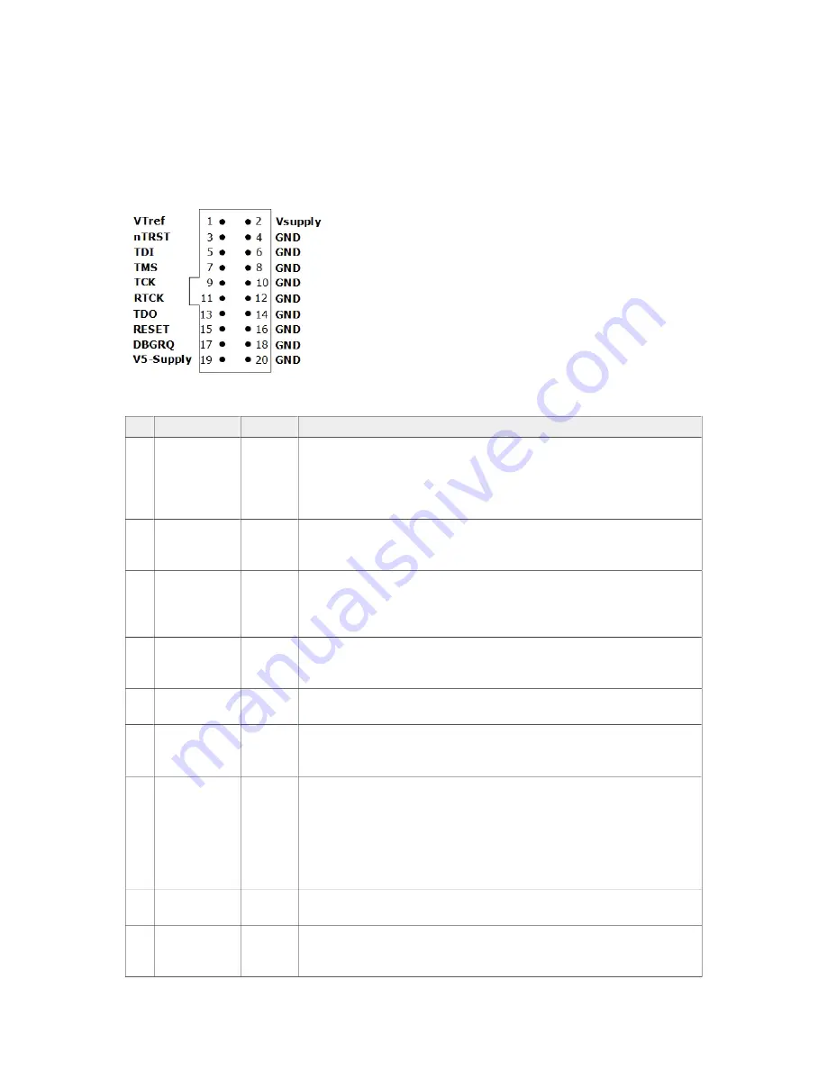
Flasher ARM 20-pin JTAG/SWD Connector
9.1 Flasher ARM 20-pin JTAG/SWD Connector
Flasher has a JTAG connector compatible with ARM’s Multi-ICE. The JTAG connector is a
20 way Insulation Displacement Connector (IDC) keyed box header (2.54mm male) that
mates with IDC sockets mounted on a ribbon cable.
9.1.1 Pinout JTAG
The following table lists the Flasher JTAG pinout.
PIN
SIGNAL
TYPE
Description
1
VTref
Input
This is the target reference voltage. It is used to check if the
target has power, to create the logic-level reference for the
input comparators and to control the output logic levels to
the target. It is normally fed from Vdd of the target board
and must not have a series resistor.
2
Vsupply
NC
This pin is not connected to Flasher ARM. It is reserved for
compatibility with other equipment. Connect to Vdd or leave
open in target system.
3
nTRST
Output
JTAG Reset. Output from Flasher ARM to the Reset signal of
the target JTAG port. Typically connected to nTRST of the
target CPU. This pin is normally pulled HIGH on the target to
avoid unintentional resets when there is no connection.
5
TDI
Output
JTAG data input of target CPU. It is recommended that this
pin is pulled to a defined state on the target board. Typically
connected to TDI of target CPU.
7
TMS
Output JTAG mode set input of target CPU. This pin should be pulled
up on the target. Typically connected to TMS of target CPU.
9
TCK
Output
JTAG clock signal to target CPU. It is recommended that this
pin is pulled to a defined state of the target board. Typically
connected to TCK of target CPU.
11 RTCK
Input
Return test clock signal from the target. Some targets must
synchronize the JTAG inputs to internal clocks. To assist in
meeting this requirement, you can use a returned, and re-
timed, TCK to dynamically control the TCK rate. Flasher ARM
supports adaptive clocking, which waits for TCK changes to
be echoed correctly before making further changes. Connect
to RTCK if available, otherwise to GND.
13 TDO
Input
JTAG data output from target CPU. Typically connected to
TDO of target CPU.
15 RESET
I/O
Target CPU reset signal. Typically connected to the RESET
pin of the target CPU, which is typically called “nRST”,
“nRESET” or “RESET”.
Flasher ATE User Guide (UM08035)
© 2017-2018 SEGGER Microcontroller GmbH
Содержание Flasher ATE
Страница 4: ...4 Flasher ATE User Guide UM08035 2017 2018 SEGGER Microcontroller GmbH...
Страница 6: ...6 Flasher ATE User Guide UM08035 2017 2018 SEGGER Microcontroller GmbH...
Страница 20: ...20 CHAPTER 2 Setting up the IP interface Flasher ATE User Guide UM08035 2017 2018 SEGGER Microcontroller GmbH...
Страница 22: ...22 CHAPTER 2 Operating modes Flasher ATE User Guide UM08035 2017 2018 SEGGER Microcontroller GmbH...
Страница 60: ...60 CHAPTER 8 ASCII command interface Flasher ATE User Guide UM08035 2017 2018 SEGGER Microcontroller GmbH...


