COMe-cWL6 – User Guide Rev. 1.4
www.kontron.com
// 24
2.3.3.2.
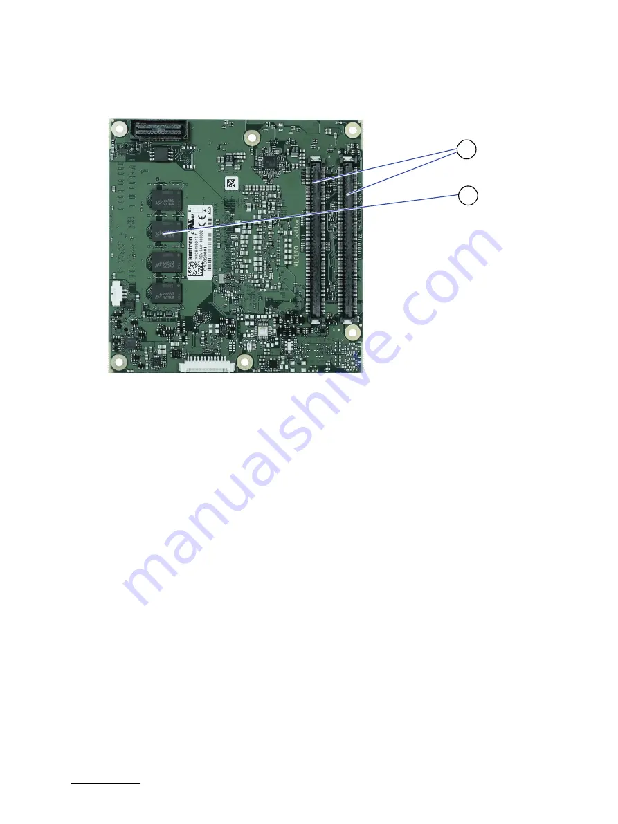
Rear View
Figure 4: Rear View COMe-cWL6
3.
2x COMe Connectors
4.
Memory down
3
4
Страница 1: ...USER GUIDE www kontron com 1 COMe cWL6 User Guide Rev 1 4 Doc ID 1065 5631...
Страница 2: ...COMe cWL6 User Guide Rev 1 4 www kontron com 2 This page has been intentionally left blank...
Страница 3: ...be suitable for the specified use without further testing or modification Kontron expressly informs the user that this user guide only contains a general description of processes and instructions whic...
Страница 4: ...quate design and operating safeguards You are solely responsible for compliance with all legal regulatory safety and security related requirements concerning your products You are responsible to ensur...
Страница 5: ...t information refer to the corporate offices contact information on the last page of this user guide or visit our website CONTACT US Customer Support Find Kontron contacts by visiting http www kontron...
Страница 6: ...cribed by the law may endanger your life health and or result in damage to your material ESD Sensitive Device This symbol and title inform that the electronic boards and their components are sensitive...
Страница 7: ...before performing any work on this product Earth ground connection to vehicle s chassis or a central grounding point shall remain connected The earth ground cable shall be the last cable to be discon...
Страница 8: ...oduct then re pack it in the same manner as it was delivered Special care is necessary when handling or unpacking the product See Special Handling and Unpacking Instruction Quality and Environmental M...
Страница 9: ...1 Module Variants 17 2 1 1 Commercial Grade Modules 0 C to 60 C 17 2 1 2 Extended Temperature Grade Modules E1 25 C to 75 C 18 2 1 3 E2S Modules E2S 40 C to 85 C 18 2 2 Accessories 19 2 3 Functional...
Страница 10: ...Kontron Heatspreader Plate HSP Assembly 39 4 4 Operating without Kontron Heatspreader Plate HSP Assembly 39 5 Environmental Specification 40 5 1 MTBF 41 6 Mechanical Specification 43 6 1 Dimensions 4...
Страница 11: ...ries 19 Table 5 COMe Type 6 Specific Accessories 19 Table 6 General Accessories 19 Table 7 Memory 20 Table 8 Technical Data 21 Table 9 8th Generation Intel Core Processors U Series Mobile U Specificat...
Страница 12: ...nu Sub screens 70 Table 52 Advanced Setup menu Sub screens and Functions 71 Table 53 Chipset menu Sub screens and Functions 76 Table 54 Security Setup Menu Functions 80 Table 55 Boot Menu Functions 82...
Страница 13: ...l successor for existing solutions as it takes over their pin assignment and feature implementation Typical applications include communication digital signage professional gaming and entertainment med...
Страница 14: ...omponent The product names for Kontron COM Express Computer on Modules consist of Short form of the industry standard COMe cWL6 Module form factor b basic 125 mm x 95 mm c compact 95mm x 95 mm m mini...
Страница 15: ...type Table 1 IOs of Type 6 and COMe cWL6 Feature Type 6 Pinout COMe cWL6 Pinout HD Audio 1x 1x Gb Ethernet 1x 1x Serial ATA 4x 2x PCI Express x 1 8x 5x PCIe 3 0 On request 6x without Ethernet up to 8...
Страница 16: ...s implements physically Designers can place connectors precisely where needed for the application on a baseboard optimally designed to fit a system s packaging A single baseboard design can use a rang...
Страница 17: ...ompact pin out type 6 Computer on Module with Intel Core i7 8665UE 4x1 7 GHz 8 GB memory down DDR4 SO DIMM Socket 36028 0000 17 7 COMe cWL6 i7 8665UE COM Express compact pin out type 6 Computer on Mod...
Страница 18: ...g process contact Kontron Support Table 3 E2S Modules E2S 40 C to 85 C operating Product Number Product Name Description 36029 8000 17 7 COMe cWL6 E2S i7 8665UE 8GB COM Express compact pin out type 6...
Страница 19: ...ght Adapter Part Number COMe Starter kit Project Code Comment 38106 0000 00 S COMe Eval Starter kit T6 Topanga Canyon Starter kit with COMe Evaluation Carrier T6 Table 6 General Accessories Part Numbe...
Страница 20: ...B_CWL6 Memory for Computer on Module COMe cWL6 min specification DDR4 2400 4 GB 260P 1200 MHz PC4 2400 SODIMM validated for COMe cWL6 97021 3224 CWL6 DDR4 2400 SODIMM 32GB E2_CWL6 Memory for Computer...
Страница 21: ...ithout Ethernet up to 8x without Ethernet SATA 4x PCIE 3 0 on PEG Lanes 0 3 USB 4x USB 3 1 Gen2 incl USB2 0 4x USB 2 0 Serial 2x UART Audio High De nition Audio Common Features SPI LPC SMB Fast I C St...
Страница 22: ...OMe cWL6 User Guide Rev 1 4 www kontron com 22 2 3 2 Block Diagram COMe cWL6 The following figure displays the system block diagram applicable to all COMe cWL6 modules Figure 2 Block Diagram COMe cWL6...
Страница 23: ...COMe cWL6 User Guide Rev 1 4 www kontron com 23 2 3 3 Front and Rear View 2 3 3 1 Front View Figure 3 Front View COMe cWL6 1 1x SO DIMM DDR4 slot 2 SoC Processor 1 2...
Страница 24: ...COMe cWL6 User Guide Rev 1 4 www kontron com 24 2 3 3 2 Rear View Figure 4 Rear View COMe cWL6 3 2x COMe Connectors 4 Memory down 3 4...
Страница 25: ...rs offer long life availability embedded use conditions Intel vPro technology on selected SKUs increased I O capacity support for Intel Optane memory and the DDR4 2400 memory These processors meet the...
Страница 26: ...y Size 64 GB 64 GB 64 GB 64 GB Independent Displays 3 3 3 3 Package FCBGA1528 FCBGA1528 FCBGA1528 FCBGA1528 2 3 5 System Memory The system memory supports a dual channel 64 bit DDR4 2400 or LPDDR3 213...
Страница 27: ...aximum display resolutions at a set frequency and bit per pixel bpp for the supported display interfaces Table 11 Display Resolution Display Interfaces Maximum Resolution Pixel eDP 4096x2304 60 Hz DP...
Страница 28: ...6 DDI2_CTRLCLK_AUX DDI2_AUXP CPU DDPC_CTRLCLK PCH DDI2_CTRLDATA_AUX DDI2_AUXN CPU DDPC_CTRLDATA PCH DDI2_DDC_AUX_SEL Connected to DDC AUX Mux DDI2_HPD DDPC_HPD1 2 3 6 3 LVDS LVDS is implemented by NX...
Страница 29: ...DS_BKLT_EN EDP_BKLTEN LVDS_BKLT_CTRL EDP_BKLTCTL 2 3 7 HD Audio The HD Audio HDA stream can be supported simultaneously on HDMI DP Table 17 Audio COMe Connector PCH HDA_RST HDA_RST HDA_SYNC HDA_SYNC H...
Страница 30: ...PROM SO DIMM A4h DDR4 Channel B SPD EEPROM memory down 30h DDR4 Channel A optional Temperature Sensor SO DIMM 5Ch Hardware Monitor 2 3 11 Wake Signals Table 19 Wake Signals COMe Signal PCH Pin Descrip...
Страница 31: ...nd off module boot from SPI For additional safety a second on module SPI flash can be populated on the board This also requires an adoption of the FPGA EC code Features as SAFS together with eSPI are...
Страница 32: ...rd Fan Connector chapter 2 3 21 2 3 20 Trusted Platform Module TPM Chip is Infineon SLB9670 TPM 2 0 connected to BOOT SPI0 TPM_PP pin is connected to COMe TPM_PP pin 2 3 21 Onboard Fan Connector The a...
Страница 33: ...A0 PCIE11 x1 PCIE7 no SATA1 PCIE12 x1 PEG0 PCIE13 x1 x4 YES PEG1 PCIE14 x1 PEG2 no NVME PCIE15 x1 PEG3 no NVME no SATA2 PCIE16 x1 2 3 24 Universal Serial Bus USB For every USB 3 1 port one USB2 and on...
Страница 34: ...to 6 Gb s Table 32 SATA COMe Port PCH HSIO Function SATA0 SATA0 SATA1 SATA1A SATA2 SATA2 optional SATA3 nc 2 3 26 Ethernet Intel I219LM Ethernet Connection PHY only connected to PCH HSIO Port 10 PCIe...
Страница 35: ...oduct features Table 35 Kontron Features External I2C Bus Fast I2C 100 KHz 400 kHz MultiMaster capable Embedded API KEAPI3 Custom BIOS Settings Flash Backup Supported Watchdog Support Dual staged Exte...
Страница 36: ...voltage 10 to nominal VCC To comply with the ATX specification there must be a smooth and continuous ramp of each DC input voltage from 10 to 90 of the DC input voltage final set point 3 1 2 Power Sup...
Страница 37: ...Bus Alert SMB_ALERT Pin B15 With an external battery manager present and SMB_ALERT connected the module always powers on even if the BIOS switch After Power Fail is set to Stay Off 3 4 Power Supply Mo...
Страница 38: ...nals are not relevant for the specific power state It makes no difference if the signal is connected or open All ground pins must be connected to the carrier board s ground plane If any of the supply...
Страница 39: ...n the COM Express application and environmental conditions Active or passive cooling solutions provided from Kontron for the COMe cWL6 are usually designed to cover the power and thermal dissipation f...
Страница 40: ...frequency electromagnetic field immunity IEC EN 61000 4 4 Electrical fast transient burst immunity IEC EN 61000 4 5 Surge immunity IEC EN 61000 4 6 Immunity to conducted disturbances induced by radio...
Страница 41: ...hod 1 Case 3 in a ground benign controlled environment GB GC This particular method takes into account varying temperature and stress data and the system is assumed to have not been burned in The figu...
Страница 42: ...stimates assume no fan but a passive heat sinking arrangement Estimated RTC battery life as opposed to battery failures is not accounted for in the above figure and needs to be considered separately B...
Страница 43: ...e cWL6 User Guide Rev 1 4 www kontron com 43 6 Mechanical Specification 6 1 Dimensions The dimensions of the module are 95 0 mm x 95 0 mm 3 75 x 3 75 Figure 8 Module Dimensions All dimensions shown in...
Страница 44: ...module height of approximately 13 mm from module PCB bottom to heatspreader top as shown in Figure 9 Module Height below Figure 9 Module Height 1 Heatspreader 2 Heatspreaader standoff s 3 Module PCB...
Страница 45: ...xpress Computer On Modules imply BIOS support for the following external baseboard LPC Super I O controller features for the Winbond Nuvoton 3 3V 83627DHG P Table 41 Supported BIOS Features Winbond Nu...
Страница 46: ...acturer Part Number Device ID 8 MB Macronix MX25L6406E 0x20 7 3 Fast I2C Fast I2C supports transfer between components on the same board The COMe cWL6 features an onboard I2C controller connected to t...
Страница 47: ...pecific BIOS code handles the interrupt The current BIOS handler for the watchdog SMI currently does nothing For special requirements contact Kontron Support 0100b SCI A system control interrupt SCI i...
Страница 48: ...he CPU Each TPM chip contains an RSA key pair called the Endorsement Key EK The pair is maintained inside the chip and cannot be accessed by software The Storage Root Key SRK is created when a user or...
Страница 49: ...X1A and X1B and the first pin of row A and row D 8 1 X1A and X1B Signals For a description of the terms used in the X1A and X1B pin assignment tables see Table 45 General Signal Description or Append...
Страница 50: ...stor OA Output Analog PWR Power Connection OD Output Open Drain and Differential Pair To protect external power lines of peripheral devices make sure that the wires have the right diameter to withstan...
Страница 51: ...ND Power Ground PWR GND A12 GBE0_MDI0 Ethernet Media Dependent Interface 0 DP I O A13 GBE0_MDI0 Ethernet Media Dependent Interface 0 DP I O A14 GBE0_CTREF Center Tab Reference Voltage O 1 F capacitor...
Страница 52: ...P I O PD 14 25k to 24 8k in PCH A40 USB4 USB 2 0 Data Pair Port 4 DP I O PD 14 25k to 24 8k in PCH A41 GND Power Ground PWR GND A42 USB2 USB 2 0 Data Pair Port 2 DP I O PD 14 25k to 24 8k in PCH A43 U...
Страница 53: ...ss Lane 0 Transmit DP O A70 GND Power Ground PWR GND A71 LVDS_A0 LVDS Channel A DAT0 EDP Lane 2 Transmit DP O A72 LVDS_A0 LVDS Channel A DAT0 EDP Lane 2 Transmit DP O A73 LVDS_A1 LVDS Channel A DAT1 E...
Страница 54: ...in PCH S5 All SPI signals are tri stated with 20k ohm CPU internal weak pull up until reset is deasserted A95 SPI_MOSI SPI Master Out Slave In O 3 3 PU 15k 40k in PCH S5 All SPI signals are tri state...
Страница 55: ...5 20V protection circuit implemented on module A104 VCC_12V Main Input Voltage 4 75 20V PWR 4 75 20V A105 VCC_12V Main Input Voltage 4 75 20V PWR 4 75 20V A106 VCC_12V Main Input Voltage 4 75 20V PWR...
Страница 56: ...eSPI Master Data I O 3 I O 3 3 eSPI I O 1 8 PU 15k 40k in PCH S5 B8 LPC_DRQ0 ESPI_ALERT0 LPC Serial DMA Master Request 0 eSPI Alert 0 I 3 3 eSPI I 1 8 eSPI PU 1k 1 8V S5 B9 LPC_DRQ1 ESPI_ALERT1 LPC Se...
Страница 57: ...P I O PD 14 25k to 24 8k in PCH B37 USB7 USB 2 0 Data Pair Port 7 DP I O PD 14 25k to 24 8k in PCH B38 USB_4_5_OC USB Overcurrent Indicator Port 4 5 I 3 3 PU 10k 3 3V S5 B39 USB5 USB 2 0 Data Pair Por...
Страница 58: ...P I B66 WAKE0 PCI Express Wake Event I 3 3 PU 10k 3 3V S5 B67 WAKE1 General Purpose Wake Event I 3 3 PU 10k 3 3V S5 B68 PCIE_RX0 PCI Express Lane 0 Receive DP I B69 PCIE_RX0 PCI Express Lane 0 Receive...
Страница 59: ...ata Channel Clock nc B96 VGA_I2C_DATA Display Data Channel Data nc B97 SPI_CS SPI Chip Select O 3 3 B98 RSVD Reserved for future use nc B99 RSVD Reserved for future use nc B100 GND Power Ground PWR GN...
Страница 60: ...2 DP I C10 USB_SSRX2 USB Super Speed Receive 2 DP I C11 GND Power Ground PWR GND C12 USB_SSRX3 USB Super Speed Receive 3 DP I C13 USB_SSRX3 USB Super Speed Receive 3 DP I C14 GND Power Ground PWR GND...
Страница 61: ...c C47 DDI3_PAIR2 DDI3 Pair 2 nc C48 RSVD Reserved for future use nc C49 DDI3_PAIR3 DDI3 Pair 3 nc C50 DDI3_PAIR3 DDI3 Pair 3 nc C51 GND Power Ground PWR GND C52 PEG_RX0 PEG Lane 0 Receive DP I C53 PEG...
Страница 62: ...Power Ground PWR GND C88 PEG_RX11 PEG Lane 11 Receive nc C89 PEG_RX11 PEG Lane 11 Receive nc C90 GND Power Ground PWR GND C91 PEG_RX12 PEG Lane 12 Receive nc C92 PEG_RX12 PEG Lane 12 Receive nc C93 GN...
Страница 63: ...mit 2 DP O D10 USB_SSTX2 USB Super Speed Transmit 2 DP O D11 GND Power Ground PWR GND D12 USB_SSTX3 USB Super Speed Transmit 3 DP O D13 USB_SSTX3 USB Super Speed Transmit 3 DP O D14 GND Power Ground P...
Страница 64: ...uture use nc D49 DDI2_PAIR3 DDI2 Pair 3 DP O D50 DDI2_PAIR3 DDI2 Pair 3 DP O D51 GND Power Ground PWR GND D52 PEG_TX0 PEG Lane 0 Transmit DP O D53 PEG_TX0 PEG Lane 0 Transmit DP O D54 PEG_LANE_RV Not...
Страница 65: ...round PWR GND D91 PEG_TX12 PEG Lane 12 Transmit nc D92 PEG_TX12 PEG Lane 12 Transmit nc D93 GND Power Ground PWR GND D94 PEG_TX13 PEG Lane 13 Transmit nc D95 PEG_TX13 PEG Lane 13 Transmit nc D96 GND P...
Страница 66: ...screen POST messages or splash screen 3 Press the DEL key 4 If the UEFI BIOS is password protected a request for password will appear Enter either the User Password or Supervisor Password press RETURN...
Страница 67: ...Shell forms an entry into the UEFI boot order and is the first boot option by default 9 2 1 1 Entering the UEFI Shell To enter the UEFI Shell follow the steps below 1 Power on the board 1 Press the F7...
Страница 68: ...up script terminates then the default boot order is continued 9 3 2 Create a Startup Script Startup scripts can be created using the UEFI Shell built in editor edit or under any OS with a plain text e...
Страница 69: ...sing RETURN Each Setup menu provides two main frames The left frame displays all available functions Configurable functions are displayed in blue Functions displayed in grey provide information about...
Страница 70: ...Information Read only field Displays Module Information Product Name Revision Serial MAC Address Boot Counter and CPLD Rev Additional information for MAC Address The MAC address entry is the value use...
Страница 71: ...een to incorrect values may cause system malfunctions Figure 13 Advanced Setup Menu Table 52 Advanced Setup menu Sub screens and Functions Sub Screen Function Second level Sub Screen Description RC AC...
Страница 72: ...le Disable Intel Speed ShiftTechnology Enable Disable Turbo Mode Enable Disable View Configure Turbo Options Energy Efficient P State Enable Disable Package Power Limit MSR Enable Disable 1 Core Ratio...
Страница 73: ...Enable Disable Platform Thermal Configuration Automatic Thermal Reporting Enable Disable Critical Trip Point 119 C POR Passive Trip Point 95 C Passive TC1 value 1 Passive TC2 value 5 Passive TSP value...
Страница 74: ...le Reset Button Behavior Chipset Reset Power Cycle I2C Speed 200 Onboard I2C Mode Multimaster Busclear Lid Switch Mode Enable Disable Sleep Button Mode Enable Disable ACPI temperature polling Enable D...
Страница 75: ...e this device Enable Disable Possible Use Automatic Settings PCI Subsystem Settings BME DMA Mitigation Enable Disable USB Configuration Legacy USB Support Enable Disable XHCI Hand Off Enable Disable U...
Страница 76: ...ial Screen Table 53 Chipset menu Sub screens and Functions Function Second level Sub Screen Description System Agent Memory Configuration Memory Test on Warm Boot Enable Disable Maximum Memory Frequen...
Страница 77: ...DVI EFP3 LSPCON Enable Disable Mode Persistence Enable Disable Center Mode Enable Disable Stop Grant Conf Auto VT d Enable Disable Above 4 GB MMIO Enable Disable PCH IO Configuration PCI Express Confi...
Страница 78: ...2 3 Port 0 1 2 3 Enable Disable External Enable Disable Spin Up Device Enable Disable SATA Device Type Hard Disk Drive USB Configuration xDCI Support Enable Disable USB Overcurrent Enable Disable USB...
Страница 79: ...COMe cWL6 User Guide Rev 1 4 www kontron com 79 Function Second level Sub Screen Description PCIe P11 SSC Auto 0 0 SPD Write Disable True...
Страница 80: ...Security Setup Menu Initial Screen The following table shows the Security set up sub screens and functions and describes the content Table 54 Security Setup Menu Functions Function Description Adminis...
Страница 81: ...he user s password is set then the password is a power on password and must be entered to boot or enter setup In the setup the user has administrator rights The required password length in characters...
Страница 82: ...unctions for booting up the setup program Figure 16 Boot Screen Table 55 Boot Menu Functions Function Description Setup Prompt Timeout 1 Bootup NumLock State On Off Quiet Boot Enabled Disabled Boot Op...
Страница 83: ...Changes and Exit Exits system setup without saving changes Save Changes and Reset Resets system after saving changes Discard Changes and Reset Resets system setup without saving changes Save Changes S...
Страница 84: ...Addition connected hardware full description of hardware set up The serial number can be found on the Type Label located on the product s rear side Be ready to explain the nature of your problem to th...
Страница 85: ...or Kontron Europe GmbH and fill out the form Take care to include a short detailed description of the observed problem or failure and to include the product identification Information Name of product...
Страница 86: ...ble Unit Gb Gigabit GBE Gigabit Ethernet GPI General Purpose Input GPIO General Purpose Input Output GPO General Purpose Output GPU Graphics Processing Unit HBR2 High Bitrate 2 HDA High Definition Aud...
Страница 87: ...all Outline Dual in line Memory Module SOIC Small Outline Integrated Circuit SOL Serial Over LAN SPI Serial Peripheral Interface SSH Secure Shell TPM Trusted Platform Module UART Universal Asynchronou...
Страница 88: ...ts and tailor made solutions based on highly reliable state of the art embedded technologies Kontron provides secure and innovative applications for a variety of industries As a result customers benef...