OfficeServ 7100 Service Manual
© SAMSUNG Electronics Co., Ltd.
2-17
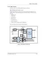
The voice signal transmitted to the transformer secondary side is separated into the Tx path
and the Rx path at the Impedance matching & Balance circuit. In addition, it matches the
resistance to 600 600
Ω
and embeds the low frequency compensation function in the low
frequency Impedance matching & Balance circuit. At present, it is designed in Long Loop
Impedance Matching method. The converted Tx voice signal is converted into Pulse Code
Modulation(PCM) data by the digital coding of CODEC and assigned to the corresponding
channel. After that, the signal is transmitted to the time switch through the PCM highway and the
digital gain control circuit. The Rx PCM data, which are the Rx voice signal, is converted into
an analog signal by CODEC. The converted signal is transmitted to the Balancing circuit
through the Impedance Matching circuit. Only the received voice signal is supplied tio the
transformer secondary side again and transmitted to the line feeding power. This signal is
matched with the voice path of the C.O. line interface. As mentioned above, the voice
signal is transmitted in the different path from the transmission path.
Ring Reception Detection Circuit
The ring reception signal transmitted from the C.O. switch is transmitted as the incoming
signal when the C.O. interface is in Hook-on mode. The DC voltage of the ring signal is cut
off by the Poly-capacitor of 0.47 uF/250 V on the normal contact of the loop relay.
After that, only the ring signal of more than a certain level passes the bridge diod.
Now, this signal is entered to the photo-coupler through a resistance to generate the ring
detection signal. In normal mode, the ring detection signal becomes ‘L’. However, the signal
becomes ‘H’ when the ring is transmitted.
DC Current By-pass Circuit
The DC Current by-pass circuit occupies the DC loop of the C.O. circuit and passes AC
signals. To minimize the mounting area, this circuit is established as a hybrid ID.
When both ends of Tip and Ring constructs a loop at -54 V, the circuit makes a DC path
and fixes the resistance to 33
Ω
to satisfy 30 mA/6 V, which is the specified value.
In addition, the circuit supplies Hook-off Sensing(HOS) output, which is the loop detection
function, to the system via the photo-coupler until the loop is occupied. The signal changed
into ‘L’ from ‘H’ of the normal HOS mode is detected. The circuit reverses the signal and
transmits to the CPU ata bus.
Содержание OFFICESERV 7100
Страница 1: ...Ed 00 OfficeServ 7100 Service Manual ...
Страница 33: ...OfficeServ 7100 Service Manual SAMSUNG Electronics Co Ltd 1 15 ...
Страница 189: ...OfficeServ 7100 Service Manual SAMSUNG Electronics Co Ltd 5 3 Soldering Side ...
Страница 191: ...OfficeServ 7100 Service Manual SAMSUNG Electronics Co Ltd 5 5 5 3 4DLM Part Side Soldering Side ...
Страница 193: ...OfficeServ 7100 Service Manual SAMSUNG Electronics Co Ltd 5 7 5 5 4SLM Part Side Soldering Side ...
Страница 195: ...OfficeServ 7100 Service Manual SAMSUNG Electronics Co Ltd 5 9 5 7 TEPRI2 Board Part Side ...
Страница 197: ...OfficeServ 7100 Service Manual SAMSUNG Electronics Co Ltd 5 11 5 8 8COMBO Part Side ...
Страница 199: ...OfficeServ 7100 Service Manual SAMSUNG Electronics Co Ltd 5 13 5 9 16DLI2 Part Side ...
Страница 201: ...OfficeServ 7100 Service Manual SAMSUNG Electronics Co Ltd 5 15 5 10 MGI16 MGI32 Part Side ...
Страница 203: ...OfficeServ 7100 Service Manual SAMSUNG Electronics Co Ltd 5 17 5 11 16SLI2 16MWSLI Part Side ...
Страница 205: ...OfficeServ 7100 Service Manual SAMSUNG Electronics Co Ltd 5 19 5 12 8TRK Board Part Side ...
Страница 207: ...OfficeServ 7100 Service Manual SAMSUNG Electronics Co Ltd 5 21 5 13 PLIM Board Part Side ...
Страница 209: ...OfficeServ 7100 Service Manual SAMSUNG Electronics Co Ltd 5 23 5 14 Modem Part Side Soldering Side ...


