GSM/GPRS/GNSS Module Series
MC60 Series Hardware Design
MC60_Series_Hardware_Design Confidential / Released 75 / 114
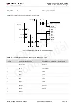
In order to enhance the reliability and availability of the SD card in applications, please follow the criteria
below in SD card circuit design:
Keep all the SD card signals far away from RF and VBAT traces.
Make sure the length of SD card signal lines does not exceed 10cm and be as short as possible.
The traces of SD_CLK, SD_DATA and SD_CMD are recommended to be routed together and be of
equal length; the length difference should be less than 10mm.
In order to offer good ESD protection, it is recommended to add a TVS diode array whose parasitic
capacitance should be not more than 50pF, and should be placed as close as possible to the SD
card connector.
Reserve external pull-up resistors for other data lines except the DATA0 signal.
The SD_CLK and SD_DATA traces are recommended to be shielded by ground in order to improve
EMI suppression capability and prevent the crosstalk.
3.14. ADC
The module provides an ADC channel to measure the value of voltage. Please give priority to the use of
ADC channel. Command
AT+QADC
can read the voltage value applied on ADC pin. For details of this AT
command, please refer to
document [1]
.
In order to improve the accuracy of ADC, the layout of ADC
should be surrounded by ground.
Table 28: Pin Definition of the ADC
Table 29: Characteristics of the ADC
Pin Name
Pin No.
I/O
Description
ADC
6
AI
Analog-to-digital converter
Item
Min.
Typ.
Max.
Unit
Voltage Range
0
2.8
V
ADC Resolution
10
bits
ADC Accuracy
2.7
mV
Quectel
Confidential

