P a y R a n g e | B l u K e y P r o | U s e r M a n u a l
P a g e
20 | 23
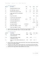
4.
Operating Conditions
Symbol
Description
Min
Typ
Max
Unit
T
O
Operating temperature range
‐30
‐
85
°C
V
CC
AC1/GND Power supply, DC
9
12
50
VDC
V
CC
AC1/AC2 Power supply, AC (rms)
16
24
29
VAC
I
CC
Power supply current, max (@ 9VDC or
16VAC)
‐
‐
575
mA
U
CC
Power consumption
‐
‐
3.8
W (1)
V
DDO
5V_OUT power supply output, DC
‐
+5.0
‐
V
V
DDI
5V_IN power supply input, DC
+1.65
+5
+5.5
V
I
DDI
5V_IN power supply input, DC
‐
‐
62
mA
V
IL
Input logic level low
V
DD
*0.4
V (2)
V
IH
Input logic level high
V
DD
*0.6+0.4
‐
‐
V (2)
V
OH
Output high voltage (I
O
= ‐32mA)
V
DD
‐0.7
‐
‐
V (2)
V
OL
Output low voltage (I
O
= +32mA)
‐
‐
0.55
V
1.
Power consumption excludes load on AC1/AC2/DC_OUT by connected card reader.
2.
VDD is 5V_OUT on MACHINE connector, and 5V_IN on CARD connector.
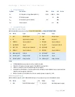
5.
ESD handling ratings
Symbol
Description
Min.
Max.
Unit Notes
V
HBM
Electrostatic discharge voltage,
human body model
‐2000
+2000
V
1
V
CDM
Electrostatic discharge voltage,
charged‐device model
‐500
+500
V
2
I
LAT
Latch‐up current at ambient temperature of
105°C
‐100
+100
mA
3
1.
Determined according to JEDEC Standard JESD22‐A114, Electrostatic Discharge (ESD) Sensitivity
Testing Human Body Model (HBM).
2.
Determined according to JEDEC Standard JESD22‐C101, Field‐Induced Charged‐Device Model
Test Method for Electrostatic‐Discharge‐Withstand Thresholds of Microelectronic Components.
3.
Determined according to JEDEC Standard JESD78, IC Latch‐Up Test.


