


Advanced Chipset Features
13
Advanced Chipset Features
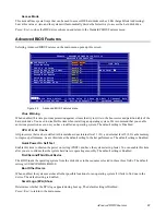
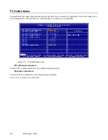
This option displays critical timing parameters of the mainboard. Leave the items on this menu at their default settings
unless you are very familiar with the technical specifications of the system hardware. If you change the values incor-
rectly, you may introduce fatal errors or recurring instability into the system.
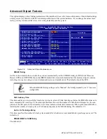
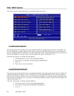
Figure 2.6
Advanced Chipset Features menu
DRAM Timing
Set this to the default value to enable the system to automatically set the SDRAM timing by SPD (Serial Presence
Detect). SPD is an EEPROM chip on the DIMM module that stores information about the memory chips it contains,
including size, speed, voltage, row and column addresses, and manufacturer. The default value is By SPD.
CAS Latency Time
This item enables you to specify the time delay (in clock cycles or CLKs) that elapses before the SDRAM carries out a
read command after receiving it. The value specified here also sets the number of CLKs that will elapse for the com-
pletion of the first part of a burst transfer. Low values indicate a faster data transaction. When synchronous DRAM is
installed, the number of clock cycles of CAS latency depends on the DRAM timing. The default is 2.5.
Active to Precharge Delay
This item specifies the number of clock cycles needed after a bank active command before a precharge can occur. The
default is 6.
DRAM RAS# to CAS# Delay
The default is 3.
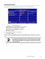
NOTE
When the DRAM Timing setting is set to “Manual”, the fields preceded by an “x” becomes
configurable.
P
hoenix – AwardBIOS CMOS Setup Utility
Advanced Chipset Features
DRAM Timing Selectable
[By SPD]
x CAS Latency Time
2.5
Item Help
x Active to Precharge Delay
6
x DRAM RAS# to CAS# Delay
3
Menu Level
`
x DRAM RAS# Precharge
3
DRAM Integrity Mode
Non-ECC
MGM Core Frequency
400/266/133/200 MHz
System BIOS Cacheable
[Enabled]
Video BIOS Cacheable
[Disabled]
Memory Hole at 15M-16M
[Disabled]
**On=Chip VGA Setting**
On-Chip Frame Buffer Size
[32MB]
Boot Display
CRT+LFP
Panel Number
1024x768 24Bit/1CH
ÇÈÅÆ
:Move Enter:Select +/-/PU/PD:Value F10:Save ESC:Exit F1:General Help
F5: Previous Values F6: Fail-Safe Defaults F7: Optimized Defaults
Содержание PT-6900
Страница 1: ...PT 6900 Service Manual...
Страница 2: ......
Страница 7: ...v List of Parts FRUs 92 Display Parts and Cables 94...
Страница 8: ...vi...
Страница 10: ...viii...
Страница 16: ...6 Getting Started...
Страница 38: ...28 BIOS Setup Utility...
Страница 52: ...42 Installing Drivers and Software 5 When installation is completed click Finish...
Страница 66: ...56 Locating the Problem...
Страница 83: ...Replacing Parts 73 6 Remove the touch panel 7 Remove the waterproof seal...
Страница 88: ...78 Replacing Field Replaceable Units FRUs...
Страница 96: ...86 Appendix Optional Components Exploded Diagram and Parts List...
Страница 106: ...96 Appendix Optional Components Exploded Diagram and Parts List...