background image

TEST AND MEASUREMENT

MCUK000601C8

Section 6

Issue 1

Service Manual

– 41 –

Revision 0

6.6. Adjustment Mode

6.6.1.

RF Calibration Procedure

NOTE:

See Section 6.2 for a list of the equipment and setup procedures required  to perform the following adjustment
and calibration procedures.

The following procedures MUST be performed after replacement or repair of one or both of the PCBs in the handheld unit.  
Failure to do so may result in incorrect operation of the telephone.

The following adjustments MUST be made on BOARD PAIRS.

There are three distinct calibration procedures to adjust RF performance. These procedures are:

1.

Ramping gain (Section 6.6.1)

2.

RSSI (Section 6..6.2)

3.

I and Q values (Section 6.6.3)

The adjustment data selected during calibration is stored in Flash ROM.

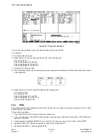
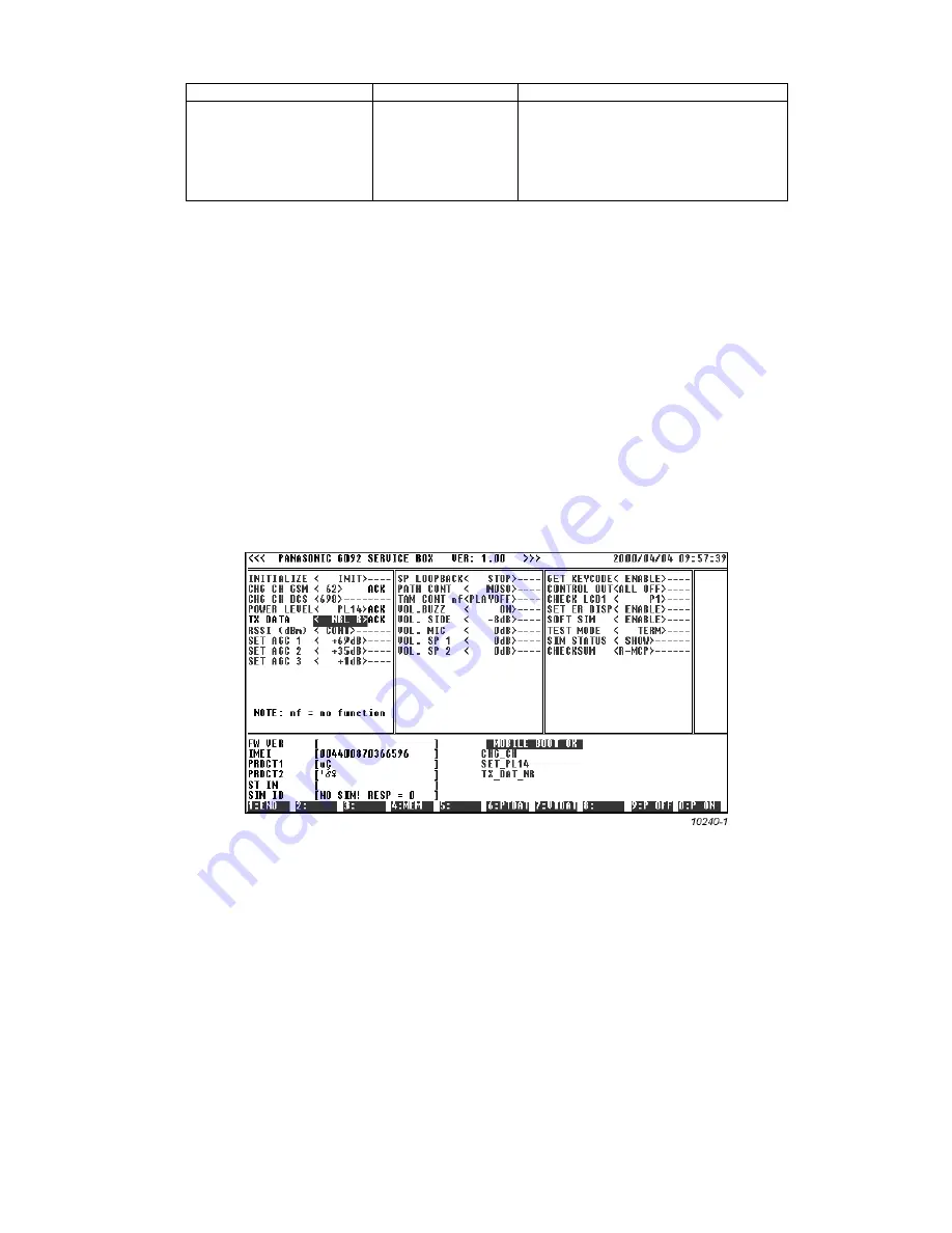
Figure 6.13:  Test software screen

6.6.2.

Ramping Gain

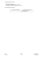
The carrier power must be measured and calibrated for each power level at channel 62.

GSM 900

NOTE: To ensure that the telephone operates within set SAR margins, Panasonic recommends that a power meter

capable of measurement to an accuracy of ±0.2 dB is used when calibrating power levels.  Use of a less
accurate power meter may result in the telephone failing to meet SAR standards.

1.

Power on the telephone in Test Set Mode.

2.

Scroll down the menu until CHANGE CH <62> is highlighted and then press ENTER.

3.

Scroll down the menu until PL <5> is highlighted. Use the left and right cursor keys to select <14>. Press ENTER.

4.

Scroll down the menu until TX DATA <OFF> is highlighted. Using the left / right cursor keys, highlight <NRL R> and press 
ENTER.

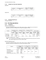
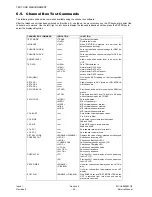
TEST MODE

<TERM>

With SOFT SIM <ENABLED> the UUT will be
removed from test mode and can be placed into a
call

SIM STATUS

<SHOW>

Checks and displays the SIM status

CHECK SUM

<SHOW>

Displays the software checksum

CHANNEL BOX COMMAND

INDICATION

FUNCTION

Содержание EB-GD52

Страница 1: ...phical chip on glass liquid crystal Alphanumeric 16 x 3 characters GD52 16 x 4 characters GD92 92C 5 icons and 6 x 1 characters Illumination 4 LEDs for the LCD Green 8 LEDs for the keypad Green 1 LED Incoming call Green 1 Charging LED Red Keypad 17 keys Navigation key SIM Plug in type only External DC Supply Voltage 5 8 V Battery GD52 3 6V nominal 600mAh NiMH GD92 92C 3 7 V nominal 650mAh Li Ion S...

Страница 2: ...ation Industrial UK Ltd accepts no responsibility for inaccuracies which may occur and reserves the right to make changes to specification or design without prior notice The information contained in this manual and all rights in any designs disclosed therein are and remain the exclusive property of Matsushita Communication Industrial UK Ltd Other patents applying to material contained in this publ...

Страница 3: ...teries This equipment may contain an internal battery in addition to the external battery packs These batteries are recyclable and should be disposed of in accordance with local legislation They must not be incinerated or disposed of as ordinary rubbish WARNING The equipment described in this manual contains polarized capacitors utilising liquid electrolyte These devices are entirely safe provided...

Страница 4: ...Issue 1 iv MCUK000601C8 Revision 0 Service Manual This page is left intentionally blank ...

Страница 5: ...ons for unpacking installing and operating the equipment 3 Servicing information provides complete instructions for the testing disassembly repair and reassembly of each major component part Step by step troubleshooting information is given to enable the isolation and identification of a malfunction and thus determine what corrective action should be taken The test information enables verification...

Страница 6: ...INTRODUCTION Issue 1 Section 1 MCUK000601C8 Revision 0 2 Service Manual This page is intentionally blank ...

Страница 7: ... and Enhanced Full Rate EFR speech codec 2 Dual Band GSM 900 and GSM 1800 operation 3 Tegic T9 Text Entry 4 Voice Ringer 5 Desktop Handsfree function comprising integral echo cancellation and noise suppression 2 2 2 GD92 and GD92C In addition GD92 and GD92C have the following features 1 E Mail access via Point to Point Protocol PPP 2 Voice Command dialling 3 Backup Battery 4 Four background displa...

Страница 8: ...ITEM DESCRIPTION PART NUMBER 1 Main Unit GD92 EB GD92 2 Battery Standard EB BSD92B Blue or EB BSD92T Titanium 3 AC Adaptor EB CAD92 Documentation See Section 7 ITEM DESCRIPTION PART NUMBER 1 Main Unit GD92C EB GD92C 2 Battery Standard EB BSD92B Blue or EB BSD92T Titanium 3 AC Adaptor EB CAD92 Documentation See Section 7 ...

Страница 9: ...ad Displays the battery charge level Battery is at full charge Battery requiresl charging The battery icon flashes during charging During car mount use when the battery is fully charged the icon will not light Menu Icon Displays a small icon related to the current status of the telephone telephone is roaming on a non home network using the Call Divert feature or the telephone has Call Divert set s...

Страница 10: ... Changes the type of characters entered during Alpha Entry Send Key Makes a call Clear Key Clears the last digit entered clears all digits when pressed and held or returns to the previous display End Key Ends a call or switches the telephone on off when pressed and held to Digit keys Enter wild numbers or pauses when pressed and held Where appropriate the 0 key scrolls up or down through abbreviat...

Страница 11: ...y is pressed for a short time the cursor will move to the next position To cycle between Greek characters extended characters W numerals X and normal characters U press 3 5 2 Editing Alpha Entry Pressing will move the cursor up or down one line Pressing will move the cursor left or right one character When the cursor is moved over a character and another key pressed this will insert the new charac...

Страница 12: ...pplications Clock Function Calculator Currency Browse Create Alert Profile Group Setting Review My Numbers Service Dial Hot Key Dial Personal Dial Speed Dial Received List Send List Create User Defined Msg Review Parameters Broadcasts Receive Message List Topics Languages Security Network Call Divert Call Service Last Call All Calls Call Waiting Caller s ID Withhold ID Call Charge Voice Calls Fax ...

Страница 13: ... Security Change PIN 0 4 OLD PIN NEW PIN NEW PIN Change PIN2 0 4 2 OLD PIN2 NEW PIN2 NEW PIN2 Unblock PIN 0 5 PIN UNBLOCKING KEY NEW PIN NEW PIN Unblock PIN2 0 5 PIN2 UNBLOCKING KEY NEW PIN2 NEW PIN2 3 9 5 Call Hold Place a Call on Hold 2 SND Recall a Held Call 2 SND Make a Second Call TELEPHONE NUMBER SND Swap between two Held Calls 2 SND End Held Call 0 SND End Active Call 1 SND Reject Incoming ...

Страница 14: ...chronous services 21 All synchronous services 22 All data synchronous services 24 All data asynchronous services 25 All dedicated packet access 26 All dedicated PAD access 27 Call Divert Type Service Code Divert all calls 21 Divert all calls if busy 67 Divert calls if no reply 61 Divert if not reachable 62 Set except No Reply Call Bar SERVICE CODE FORWARD TELEPHONE NUMBER TELECOMMUNICATION SERVICE...

Страница 15: ...attery Pack use the telephone until the Low Battery Warning appears and then fully recharge three times However if the battery life still is short the battery pack has eventually worn out Replace with a new one The battery level indicator does not light when charging If a battery is deeply discharged it will take a short time before there is sufficient power in the telephone to light the battery l...

Страница 16: ... SIM Error The telephone has detected a problem with the SIM Switch the telephone off and then back on If the message does not disappear contact the Service Provider Message Rejected Store Full A message has been received but the message store is full To receive messages delete some of the currently stored messages or set messages to automatically clear Menu Messages Parameters Auto Delete PIN2 In...

Страница 17: ...to enter the enable disable menu 3 13 4 Disabling Procedure 3 13 5 Enabling Procedure Key Sequence Notes Can only disable personalisation Can both enable and disable personalisation 1 or 2 to point at SIM for SIM Personalisation Network for Network Personalisation Subnetwork for Subnetwork Personalisation SP for Service Provider Personalisation or Corporate for Company Personalisation 3 4 the 16 d...

Страница 18: ...TA MOBILAND 213 03 GSM 900 ARMENIA 374 ARMGSM RA ARMGSM 283 01 GSM 900 AUSTRALIA 61 MOBILENET TELSTRA 505 01 GSM 900 OPTUS Mobile Yes Optus 505 02 GSM 900 VODAFONE AUS VODAFONE 505 03 GSM 900 AUSTRIA 43 A max A max 232 03 GSM 900 A1 A1 232 01 GSM 900 one one 232 05 GSM 1800 AZERBAIJAN 994 AZERCELL GSM AZE AZERCELL GSM 400 01 GSM 900 BAHREIN 973 MOBILE PLUS BHR MOBILE PLUS 426 01 GSM 900 BELGIUM 32...

Страница 19: ...Y SUNDAY 454 16 GSM 1800 HUNGARY HUNGARY HUNGARY 36 PANNON GSM H PANNON GSM 216 01 GSM 900 Vodafone Vodafone 216 70 not known WESTEL 900 H WESTEL 900 216 30 GSM 900 ICELAND 354 Postur og simi IS SIMINN 274 01 GSM 900 INDIA 91 AirTel INA AIRTL 404 10 GSM 900 BPL MOBILE BPL MOBILE 404 21 GSM 900 BPL MOBILE BPL MOBILE 404 27 GSM 900 BPL MOBILE BPL MOBILE 404 43 GSM 900 BPL MOBILE BPL MOBILE 404 46 GS...

Страница 20: ...T TELFORT 204 12 GSM 1800 NEW_ZEALAND 64 BELLSOUTH BELLSOUTH NZ 530 01 GSM 900 NORWAY 47 NetCom GSM N NetCom GSM 242 02 GSM 900 Telenor Mobile N Telenor Mobil 242 01 GSM 900 OMAN 968 OMAN MOBILE OMAN MOBILE 422 02 GSM 900 PHILLIPINES 63 Globe Telecom PH GLOBE 515 02 GSM 900 Islacom ISLACOM 515 01 GSM 900 PHILLIPINES Smart Communications SMART 515 03 GSM 1800 POLAND 48 ERA GSM PL ERA GSM 260 02 GSM...

Страница 21: ...466 93 GSM 900 TUNTEX TUNTEX 466 06 GSM 1800 TWN GSM TWN GSM 466 97 GSM 1800 TransAsia Telecom GSM TransAsia GSM 466 99 GSM 900 TANZANIA 255 Tritel TZ Tritel TZ 640 01 GSM 900 THAILAND 66 AIS GSM TH AIS GSM 520 01 GSM 900 HELLO HELLO 520 10 GSM 1800 WP 1800 WP 1800 520 18 GSM 1800 TURKEY TURKEY 90 PTT TELSIM GSM TR TELSIM 286 02 GSM 900 PTT TURKCELL GSM TR TURKCELL 286 01 GSM 900 UKRAINE 380 GOLDE...

Страница 22: ... operator Password Used for the control of the call bar function Supplied by the service provider PIN Personal Identification Number used for SIM security Supplied by the service provider PIN2 Personal Identification Number used for the control of Fixed Dial Memory and call charge metering Supplied by the service provider PUK PUK2 PIN PIN2 Unblocking Key Used to unblock the PIN PIN2 Supplied by th...

Страница 23: ... which has an integral safety resistor of between 5k2 and 1M2 shall be used Containers All containers and storage must be of the conductive type 4 2 Disassembly 4 2 1 Case Removal GD52 1 Remove the battery cover by pushing it towards the base of the phone and then lifting it away from the case Figure 4 1 GD52 Battery Cover Removal 2 Slide the battery lock to the release position and lift the batte...

Страница 24: ...igure 4 3 GD52 Case Screw Removal 4 Remove the cover from the case by pulling from the connector end of the telephone Care must be taken when separating the case from the cover as the retaining clips may be very stiff if necessary re attach the battery cover to provide extra support for the case Figure 4 4 GD52 Case Cover Separation 5 Remove the PCB assembly from the cover 10235 1 10234 1 10236 1 ...

Страница 25: ...s located inside the battery compartment Figure 4 6 GD92 GD92C Screw Removal 2 Remove the cover from the case by pulling from the connector end of the telephone Care must be taken when separating the case from the cover as the retaining clips may be very stiff If necessary re attach the battery to provide extra support for the case Figure 4 7 GD92 GD92C Case Cover Separation 3 Remove the PCB assem...

Страница 26: ...ty when replacing the battery Figure 4 9 Backup Battery Polarity 4 2 4 Access to Printed Circuit Boards All 1 Remove the case as described for the relevant product GD52 or GD92 GD92C While applying slight pressure to the side retaining clips lift the Main PCB away from the chassis Figure 4 10 Main PCB Removal 2 While applying slight pressure to the side retaining clips slide the Keypad PCB towards...

Страница 27: ... Figure 4 12 LCD Removal 4 The Light Guide and Reflector can be removed in turn by prising one side away from the chassis 4 2 5 Case Mounted Components 1 Remove the keypad membrane by peeling it away from the case front Figure 4 13 Keypad Membrane Removal 2 Remove the microphone assembly by prising upward with a small screwdriver blade or similar blunt object through the slot in the side of the mi...

Страница 28: ... similar blunt object Figure 4 16 Removal of RF Shield 5 Once the RF Shield has been removed the Memo button GD92 GD92C and Desktop Handsfree DTHF speaker may be lifted out from the case 6 The Vibrate motor may be removed by gently applying pressure under the spindle counterweight Figure 4 17 Removal of Vibrate Motor 7 Using a small screwdriver blade or similar blunt object depress the lug on the ...

Страница 29: ...moval 4 3 Re assembly Re assembly is the reverse of disassembly except that the Keypad PCB should be located in the chassis guides adjacent to the base I O connector before sliding it in to its normal location Ensure that the securing screws are not over tightened as this may affect the operation of the keypad 10228 1 ...

Страница 30: ...DISASSEMBLY REASSEMBLY INSTRUCTIONS Issue 1 Section 4 MCUK000601C8 Revision 0 26 Service Manual This page is intentionally blank ...

Страница 31: ...t Antenna Connector Offset from Centre Frequency kHz Maximum Level Relative to Carrier dB 100 200 250 600 to 1800 0 5 30 33 60 Offset from Centre Frequency kHz Maximum Level dBm GSM 900 GSM 1800 400 19 22 600 21 24 1200 21 24 1800 24 27 Frequency Range Frequency Offset Filter Bandwidth Approximate Video Bandwidth Limits dBm GSM 900 GSM 1800 30 to 50 MHz 10 kHz 30 kHz 36 36 50 to 500 MHz 100 kHz 30...

Страница 32: ...ng to the propagation conditions Power Control Level Transmitter Output Power dBm Tolerance for Conditions dB Normal Extreme TBA Power Control Level Transmitter Output Power dBm Tolerance for Conditions dB Normal Extreme TBA Channels Propogation Conditions TUhigh Propogation Conditions RA Propogation Conditions HT Static Conditions Test Limit error rate Minimum No of samples Test Limit error rate ...

Страница 33: ...Test Limit error rate Minimum No of samples Test Limit error rate Minimum No of samples Test Limit error rate Minimum No of samples Test Limit error rate Minimum No of samples TCH FS FER 4 478 α 13400 0 122 α 164000 class Ib RBER 0 32 α 1 500 000 0 41 α 20 000 000 class II RBER 8 333 60 000 7 5 24000 9 333 30000 2 439 8200 Channels Propogation Conditions TUhigh Propogation Conditions RA Propogatio...

Страница 34: ...vice Manual Spurious response exceptions Six exceptions are permitted IN band 915 980 MHz 24 exceptions are permitted OUTSIDE band 915 980 MHz Intermodulation Characteristics Interferer Level f1 f2 dBm Interferer Frequencies f1 f2 49 Wanted frequency 2f1 f2 and f1 f2 800 kHz ...

Страница 35: ...l Its aramid substrate is hydrophilic i e it absorbs moisture from the air If after having absorbed moisture the ALIVH PWB is submitted to re flow or repair process moisture in the board can suddenly evaporate and cause vapour explosion Copper Foil Peel Strength Land Detachment Resistance The ALIVH PCB is slightly less resistant to copper detachment force than conventional boards Therefore it is n...

Страница 36: ...on The handset can be connected to a compatible personal computer for electronic adjustment and fault diagnosis This section provides a description of the equipment required to perform those tasks Testing and adjustment of the handheld unit can be performed with the outer case in place and the cradle connected For in depth fault finding the unit should first be disassembled as detailed in Section ...

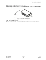
Страница 37: ...Battery Provides 3 6 V DC supply to Interface Box IFB003 or IFB004 to compensate for the current drain when the Unit Under Test is used at full transmit power Use Test Battery part number JT00045 for GD52 and part number JT00042 for GD92 and GD92C Figure 6 2 Test Battery PCB Repair Jig Part No JT00041 This unit provides the necessary connections between the Main and Keypad PCBs and the connections...

Страница 38: ... number JT00044 for GD52 and JT00040 for GD92 GD92C Figure 6 4 GD92 GD92C RF Adaptor GSM Tester This unit acts as a base station providing all the necessary GSM signalling requirements and also provides GSM signal measuring facilities Interface Cable Part No JT00043 The interface cable allows connection between a computer and the Unit Under Test via IFB003 or IFB004 Figure 6 5 Interface Cable 1026...

Страница 39: ...Control Unit BCVCU provides three voltage levels 3 V 4 1 V and 0 V to the Test Battery and is used during battery calibration checks It is powered from the Interface Box Figure 6 6 Battery Calibration Control Unit 6 3 5 Channel Box Software This is the test software for the telephone unit and should be installed onto the personal computer to be used for testing 10163 1 ...

Страница 40: ...TEST AND MEASUREMENT Issue 1 Section 6 MCUK000601C8 Revision 0 36 Service Manual 6 4 Complete Unit Setup Figure 6 7 Complete Unit Test Setup MAIN PCB KEYPAD PCB INTERNAL CONNECTOR RF CABLE 10199 1 ...

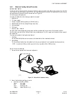
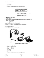
Страница 41: ... installed onto the main drive of the personal computer The RF cable is connected to the GSM test station via a suitable adapter The 12 V supply is connected to the rear socket of the Interface box Two modes are available for testing the handheld unit 1 Test Mode The Test Mode facility allows various sections of the handheld unit to be individually activated 2 Normal Mode The Normal Mode facility ...

Страница 42: ...e back light will be illuminated and all LEDs will be lit Go to Section 6 5 Channel Box Test Commands for further testing information Power On In Normal Mode 1 Connect the test equipment as shown in the diagram Figure 6 10 External test equipment setup 2 Ensure that the following settings are made a Interface box IFB003 or IFB004 Power DOWN position IGN UP position MODE UP position b Power supply ...

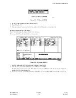
Страница 43: ...ully charged battery is attached to the telephone The screen of the PC should resemble the one shown below Figure 6 12 PC Screen SCRN11 1 At the PC change the SOFT SIM field to read ENABLE Press ENTER 2 At the PC change the TEST MODE field to read TERM Press ENTER The UUT will power down and up again If the UUT is connected to a GSM test set after a delay of approximately five seconds the UUT will...

Страница 44: ...OW MIDDLE HIGH channels SP LOOP BACK START STOP Provides an audio path for use with the GSM test station Sets audio loop back from TX audio to RX audio without processing by the CODEC PATH CONT MOSO MESI MESE MISI MISE Sets audio paths MIC off speaker off MIC external speaker internal MIC external speaker external MIC internal speaker internal MIC internal speaker external VOL BUZZ xx Sets buzzer ...

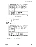
Страница 45: ...en 6 6 2 Ramping Gain The carrier power must be measured and calibrated for each power level at channel 62 GSM 900 NOTE To ensure that the telephone operates within set SAR margins Panasonic recommends that a power meter capable of measurement to an accuracy of 0 2 dB is used when calibrating power levels Use of a less accurate power meter may result in the telephone failing to meet SAR standards ...

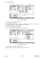
Страница 46: ...the Channel box press F7 to view the TRIM for the mid channel Figure 6 14 Power level view 1 8 Select VIEW TRIM PL MCH and make a note of this value Figure 6 15 Power level 2 9 Perform the following calculation and make a note of the result New Trim Value Old TrimValue Required Power Measured Power x Change per dB step 5 table step 2 table 10 At the Channel box press F6 to program the TRIM for the...

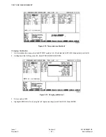
Страница 47: ...REMENT MCUK000601C8 Section 6 Issue 1 Service Manual 43 Revision 0 Figure 6 16 Power level selection 1 11 Select PROGRAM TRIM PL MCH GSM Figure 6 17 Power level selection 2 12 Highlight the PL14 fieldand press ENTER ...

Страница 48: ...00 settings in the following order PL10 limits 0 5 dB PL1 PL5 and PL15 Power levels between PL1 and PL4 Power levels between PL15 and PL10 Power level PL0 limits 0 2 dB 6 6 3 RSSI This procedure describes the calibration of RSSI on the mid channel This procedure must also be carried out for low bottom channel and high top channel The procedure is as follows 1 Power the GD92 into Test Set mode in t...

Страница 49: ...asured power is not 90 1 then make the following calculation RSSI offset value 90 MEASURED RSSI VALUE x 2 90 MEASURED RSSI VALUE x 2 for example 90 95 x 2 90 95 x 2 10 Record the result 7 At the channelbox press F7 to view data Figure 6 20 RSSI reading 1 8 Select TRIM OTHER and make a note of the RSSI COMP GSM reading ...

Страница 50: ...ogram data Figure 6 22 RSSI reading 3 11 Select TRIM RSSI and press ENTER 12 Highlight RSSI Mch GSM and press ENTER 13 Make the following calculation RSSI Offset Value step 8 reading noted in step 6 Enter the result in to the RSSI Mch field 14 Press ENTER 15 Press ESC 16 Measure the RSSI level again by highlighting the RSSI dBm field again and press ENTER ...

Страница 51: ...nal input of 33 dBm If not an appropriate attenuator must be used I Q ch Offsets Spectrum analyser setup Centre frequency 902 4 MHz RBW 10 kHz VBW 10 kHz span 1 MHz sweep time 2 sec 1 Set the Channel box to channel 62 at power level 5 nominal burst modulated with all 1 s as shown below Figure 6 23 Channel box setup 2 On the spectrum analyser measure the image leak ratio Image leak ratio is the mea...

Страница 52: ...2 Scroll down until IQCH GAIN is highlighted Press Enter Figure 6 24 I Q data selection field1 3 Enter 1 for 0 25 dB into the data field and press ENTER Figure 6 25 I Q data selection field 2 4 Measure the image leak ratio If the image leak ratio is greater than 30 dBc the telephone is within limits If the image leak ratio is less than 30 dBc repeat steps 1 2 and 3 with the following IQ Ch gain va...

Страница 53: ...r required to caibrate previous mobile products 1 Connect the telephone test battery BCVCU and Interface Box as shown in the diagram below Figure 6 26 Battery calibration test conections 2 Set the Interface box to POWER ON IGN and EXT PWR OFF Voltage Calibration 1 Enter Test Set mode in Service Channel Box Figure 6 27 Battery calibration 1 2 Press F4 and select VIEW ADC LINES 3 Observe the ADIN1 v...

Страница 54: ...ading is outside the range 390 490 there is a fault and further investigation is required Otherwise record this value for use later 7 Press N in the repeat yes no box then press ENTER 8 Press F6 Scroll down to and select TRIM OTHER 9 Scroll down to and select BAT VOLT HIGH Enter the value recorded in step 3 Figure 6 29 Battery Calibration 3 10 Press F6 Scroll down to TRIM OTHER and press ENTER 11 ...

Страница 55: ...s highlight AADC ON and then press ENTER 3 Press F4 and select VIEW ADC LINES 4 Check the value for ADIN3 BAT TEMP If the value is outside the range 168 248 then there is a fault and further investigation is required Otherwise subtract this value from the theoretical value of 208 and record the result for later use Figure 6 31 Temperature calibration 1 5 Press N in the repeat yes no box then press...

Страница 56: ...Calibration 1 On the Interface Box ensure that the EXT PWR switch is ON Check that the BCVCU 82 Ohms switch is set to ON 2 Holding down the Shift key press F4 Select PROG CHARG DAC DATA Figure 6 33 Charging calibration 1 3 Enter a value of 439 4 Highlight CNTROL OUT and using the left right cursor keys select CHAR ON Press ENTER ...

Страница 57: ...oltage 4 2 V 7 4 mV 7 Press Shift F4 8 Scroll down and select PROG CHARG DAC DATA and enter the value calculated by subtracting the value recorded in step 6 from the initial CHARG DAC DATA value 439 9 Repeat steps 6 to 8 until the measured voltage is 4 2 V 5 mV 10 If the final value is outside the range 342 542 then there is a fault and further investigation is required Otherwise record the value ...

Страница 58: ...s calibration procedure MUST be carried out once Charging Voltage calibration has been completed 1 Press F4 and select VIEW ADC LINES Read ADIN5 CRG CURRENT and record this value Figure 6 37 ADC Calibration 2 If this value is outside the range 101 251 then there is a fault and further investigation is required Otherwise calculate the difference between the recorded value and the theoretical value ...

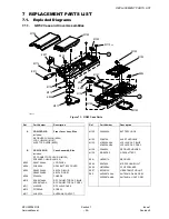
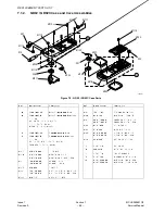
Страница 59: ...CTOR CUSHION M109 SPEAKER CUSHION M112 M103 2EA575AAAA LCD PANEL M104 2NA502A GD52 BATTERY COVER M105 2BA523AAAA 2BA523AABA KEYPAD BLUE KEYPAD GREY M108 2FA543A CHASSIS M110 6RA507AAAA 6RA507AADA RF CONNECTOR CAP BLUE RF CONNECTOR CAP GREY M111 4JA563B RF SHIELD CASE M113 3Z70054B SCREW M117 4HA532A ANTENNA CONTACT Ref Part Number Description M120 2AA5043A BATTERY HOOK M122 2QA576A ALERT LED LENS ...

Страница 60: ... 7 URQW RYHU VV OXH URQW RYHU VV 7LWDQLXP LQFOXGHV 5 9 5 86 21 0 86 21 0 57 16 0 6 6 7 DVH VVHPEO OXH DVH VVHPEO 7LWDQLXP LQFOXGHV 5 211 725 86 21 0 63 5 86 21 0 0 3 1 0 0 02 8 0 02 6 9 5 5 0 7 7 3 8 3 5 0 66 6 0 5 5 5 211 725 3 8 5 211 725 3 5 0 5 6 6 5HI 3DUW 1XPEHU HVFULSWLRQ 0 6 5 0 PP 0 17 11 217 7 0 77 5 22 8 77 5 22 5 0 1 22 635 1 0 4 57 16 0 6 3 8 6 3 5 0 5 5 9 5 2 5 5 9 5 0 523 21 81 7 6 ...

Страница 61: ...WLRQ 6HH 6HFWLRQ 0 1 2 5 66 0 3 3 3 3 66 0 0 66 6 0 4 4 7 3 3 0 5 725 6 7 3 3 17 5 2 5 211 725 3 3 7 51 5 211 725 70 211 725 2 211 725 6 62 7 QRW XVHG 94365 0 02 6 7 0 6 0 6 83 77 5 83 77 5 2 5 3 3 77 5 63 5 211 725 6 6 6 0 211 725 6 6 3 6 7 3 1 M121 M122 019 018 017 002 M108 015 010 003 016 005 008 009 B 017 x 2 011 A 10201 1 ...

Страница 62: ...GD92BRD015 MAIN PCB ACTIVA PROGRAM GD52BRD016 GD92BRD016 MAIN PCB TMN PROGRAM GD52BRD017 GD92BRD017 MAIN PCB PANNON PROGRAM GD52BRD018 GD92BRD018 MAIN PCB VODACOM PROGRAM GD52BRD019 GD92BRD019 MAIN PCB NETCOM PROGRAM GD52BRD020 GD92BRD020 MAIN PCB K P N PROGRAM GD52BRD021 GD92BRD021 MAIN PCB MOBILCOM PROGRAM GD52BRD022 GD92BRD022 MAIN PCB TELESTRA PROGRAM GD52BRD023 GD92BRD023 MAIN PCB E R A PROGR...

Страница 63: ...H100A406 CAP CER 10pF 0 5pF 50V NP0 C138 F1H1E223A029 CAP CER 22nF 10 25V X7R SMD 1 C139 ECUE1H391KBQ CAP CER 390pF 10 50V X7R SMD C141 ECUE1H101JCQ CAP CER 100pF 5 50V NP0 SMD 1 C142 F1G1A1040002 CAP CER 100nF 10 10V X7R SMD C143 ECUE1H330JCQ CAP CER 33pF 5 50V NP0 SMD 10 C144 ECUE1H151JCQ CAP CER 150pF 5 50V NP0 SMD 1 C145 ECUE1H151JCQ CAP CER 150pF 5 50V NP0 SMD 1 C146 F1G1H3R0A442 CAP CER 3pF ...

Страница 64: ...0 25pF 50V NP0 C305 ECUE1E221KBQ CAP CER 220pF 10 25V X7R SMD Model EB GD52 Name GD52 Main PCB Ref Part Number Description Notes C306 F1G1H100A406 CAP CER 10pF 0 5pF 50V NP0 C307 F1G1H100A406 CAP CER 10pF 0 5pF 50V NP0 C308 ECUE1H101JCQ CAP CER 100pF 5 50V NP0 SMD 1 C309 F3E0J1060005 CAP TANT 10uF 20 6 3V SMD CAS C310 ECUE1H101JCQ CAP CER 100pF 5 50V NP0 SMD 1 C311 F1G1E1020001 CAP CER 1nF 10 25V ...

Страница 65: ...P CER 1uF 10 6 3V X5R SMD 1 C624 F1H0J1050009 CAP CER 1uF 10 6 3V X5R SMD 1 Model EB GD52 Name GD52 Main PCB Ref Part Number Description Notes C625 F3E0G2260002 CAP TANT 22uF 20 4V SMD CASE C626 F1G1A1040002 CAP CER 100nF 10 10V X7R SMD C627 F3E1A4750001 CAP TANT 4 7uF 20 10V SMD CAS C628 ECUE1H101JCQ CAP CER 100pF 5 50V NP0 SMD 1 C629 ECUE1H101JCQ CAP CER 100pF 5 50V NP0 SMD 1 C630 F1G1H100A406 C...

Страница 66: ... 5 50V NP0 SMD 1 C704 ECUE1H101JCQ CAP CER 100pF 5 50V NP0 SMD 1 C705 F1G1A1040002 CAP CER 100nF 10 10V X7R SMD Model EB GD52 Name GD52 Main PCB Ref Part Number Description Notes C706 F1G1A1040002 CAP CER 100nF 10 10V X7R SMD C707 ECUE1H101JCQ CAP CER 100pF 5 50V NP0 SMD 1 C708 ECUE1E331KBQ CAP CER 330pF 10 25V X7R SMD C709 F1G1A1040002 CAP CER 100nF 10 10V X7R SMD C710 F1G1A1040002 CAP CER 100nF ...

Страница 67: ...X SMD FL203 EFCH225MDQA2 FILTER IF SAW 225MHz SMD J601 JC76001A CONNECTOR AUDIO JACK SKT 2 5mm Model EB GD52 Name GD52 Main PCB Ref Part Number Description Notes L101 ELJRE5N6JF2 INDUCTOR 5 6nH 5 SMD 1608 L102 G1C3N9Z00004 INDUCTOR 3 9nH 0 3nH SMD 10 L104 G1C33NJ00009 INDUCTOR 33nH 5 SMD 1005 L105 ELJRE5N6JF2 INDUCTOR 5 6nH 5 SMD 1608 L108 G1C10NJ00008 INDUCTOR 10nH 5 SMD 1005 L109 G1C5N6Z00005 IN...

Страница 68: ...M 5 1 16W SMD 1005 Model EB GD52 Name GD52 Main PCB Ref Part Number Description Notes R115 ERJ2GEJ561X RES 560 OHM 5 1 16W SMD 1005 R116 ERJ2GEJ270X RES 27 OHM 5 1 16W SMD 1005 R117 ERJ2GEJ123X RES 12K OHM 5 1 16W SMD 1005 R118 ERJ2GEJ392X RES 3 9K OHM 5 1 16W SMD 1005 R119 ERJ2GEJ392X RES 3 9K OHM 5 1 16W SMD 1005 R120 ERJ2GEJ123X RES 12K OHM 5 1 16W SMD 1005 R121 ERJ2GEJ392X RES 3 9K OHM 5 1 16W...

Страница 69: ...2 2K OHM 5 1 16W SMD 1005 R616 ERJ2GEJ222X RES 2 2K OHM 5 1 16W SMD 1005 Model EB GD52 Name GD52 Main PCB Ref Part Number Description Notes R617 ERJ2GEJ222X RES 2 2K OHM 5 1 16W SMD 1005 R618 ERJ2GEJ223X RES 22K OHM 5 1 16W SMD 1005 R619 ERJ2GEJ562X RES 5 6K OHM 5 1 16W SMD 1005 R620 ERJ2GEJ150X RES 15 OHM 5 1 16W SMD 1005 R621 ERJ2GEJ102X RES 1K OHM 5 1 16W SMD 1005 R622 ERJ2GEJ104X RES 100K OHM ...

Страница 70: ... 1A SMD 1005 R679 ERJ2GEJ103X RES 10K OHM 5 1 16W SMD 1005 R680 ERJ2GEJ104X RES 100K OHM 5 1 16W SMD 1005 R681 ERJ2GE0R00X RES JUMPER 0 OHM 1A SMD 1005 R682 ERJ2GE0R00X RES JUMPER 0 OHM 1A SMD 1005 R685 ERJ2GEJ391X RES 390 OHM 5 1 16W SMD 1005 R686 ERJ2GEJ4R7X RES 4 7 OHM 5 1 16W SMD 1005 Model EB GD52 Name GD52 Main PCB Ref Part Number Description Notes R687 ERJ2GEJ4R7X RES 4 7 OHM 5 1 16W SMD 10...

Страница 71: ...R 100nF 10 10V X5R SMD C143 ECUE1H330JCQ CAP CER 33pF 5 50V NP0 SMD 10 C144 ECUE1H151JCQ CAP CER 150pF 5 50V NP0 SMD 1 C145 ECUE1H151JCQ CAP CER 150pF 5 50V NP0 SMD 1 C146 F1G1H3R0A442 CAP CER 3pF 0 25pF 50V NP0 C148 F1G1C1030002 CAP CER 10nF 10 16V X7R SMD 1 C152 ECUE1H820JCQ CAP CER 82pF 5 50V NP0 SMD 10 C153 ECUE1H820JCQ CAP CER 82pF 5 50V NP0 SMD 10 C154 ECUE1H151JCQ CAP CER 150pF 5 50V NP0 SM...

Страница 72: ...1 C320 F1G1H100A406 CAP CER 10pF 0 5pF 50V NP0 Model EB GD92 EB GD92C Name GD92 GD92C Main PCB Ref Part Number Description Notes C321 ECUE1H101JCQ CAP CER 100pF 5 50V NP0 SMD 1 C322 F1G1H100A406 CAP CER 10pF 0 5pF 50V NP0 C323 ECUE1H101JCQ CAP CER 100pF 5 50V NP0 SMD 1 C324 ECUE1H330JCQ CAP CER 33pF 5 50V NP0 SMD 10 C350 F1G1E1020001 CAP CER 1nF 10 25V X7R SMD 10 C353 F1G1C1030002 CAP CER 10nF 10 ...

Страница 73: ... SMD 1 C647 F1G1A104A012 CAP CER 100nF 10 10V X5R SMD Model EB GD92 EB GD92C Name GD92 GD92C Main PCB Ref Part Number Description Notes C649 F1G1H150A409 CAP CER 15pF 5 50V NP0 SMD 10 C651 ECUE1H101JCQ CAP CER 100pF 5 50V NP0 SMD 1 C652 ECUE1H101JCQ CAP CER 100pF 5 50V NP0 SMD 1 C657 F1G1C3330001 CAP CER 33nF 10 16V X5R SMD 1 C658 ECUE1H330JCQ CAP CER 33pF 5 50V NP0 SMD 10 C660 F1G1C3330001 CAP CE...

Страница 74: ... DIODE MAZS0750ML ZENER 7 5V SM D609 B0BD6R800004 DIODE UMZ6 8EN ZENER 6 8V QUAD D610 B0BD6R800004 DIODE UMZ6 8EN ZENER 6 8V QUAD Model EB GD92 EB GD92C Name GD92 GD92C Main PCB Ref Part Number Description Notes D612 MAZS0750ML DIODE MAZS0750ML ZENER 7 5V SM D613 MAZS0750ML DIODE MAZS0750ML ZENER 7 5V SM D614 B0JCDD000001 DIODE RB521S 30 SCHOTTKY 30V 2 D618 MAZS0470GL DIODE MAZS0470G ZENER 4 7V SM...

Страница 75: ...R UMC3NTR PNP NPN SMD Model EB GD92 EB GD92C Name GD92 GD92C Main PCB Ref Part Number Description Notes Q601 2SD15110FL TRANSISTOR 2SD15110FL NPN HFE Q602 B1DHDC000006 TRANSISTOR SI3443DV MOSFET 20V Q603 B1GBCFNN0015 TRANSISTOR DTC144EM NPN 47K SM R101 ERJ2GEJ470X RES 47 OHM 5 1 16W SMD 1005 R102 ERJ2GEJ470X RES 47 OHM 5 1 16W SMD 1005 R104 ERJ2GEJ821X RES 820 OHM 5 1 16W SMD 1005 R105 ERJ2GEJ4R7X...

Страница 76: ...SMD 1005 R608 ERJ2GEJ121X RES 120 OHM 5 1 16W SMD 1005 Model EB GD92 EB GD92C Name GD92 GD92C Main PCB Ref Part Number Description Notes R612 ERJ2GEJ391X RES 390 OHM 5 1 16W SMD 1005 R613 ERJ2GEJ181X RES 180 OHM 5 1 16W SMD 1005 R614 ERJ2GEJ153X RES 15K OHM 5 1 16W SMD 1005 R615 ERJ2GEJ222X RES 2 2K OHM 5 1 16W SMD 1005 R616 ERJ2GEJ222X RES 2 2K OHM 5 1 16W SMD 1005 R617 ERJ2GEJ222X RES 2 2K OHM 5...

Страница 77: ... GD92 R676 ERJ2GE0R00X RES JUMPER 0 OHM 1A SMD 1005 GD92C R677 ERJ2GE0R00X RES JUMPER 0 OHM 1A SMD 1005 R678 ERJ2GE0R00X RES JUMPER 0 OHM 1A SMD 1005 R679 ERJ2GEJ103X RES 10K OHM 5 1 16W SMD 1005 R680 ERJ2GEJ104X RES 100K OHM 5 1 16W SMD 1005 R683 ERJ2GEJ104X RES 100K OHM 5 1 16W SMD 1005 R684 ERJ2GEJ472X RES 4 7K OHM 5 1 16W SMD 1005 R685 ERJ2GEJ391X RES 390 OHM 5 1 16W SMD 1005 Model EB GD92 EB ...

Страница 78: ...180 OHMx2 5 1 16W R802 EXB24V181JX RES NETWORK 180 OHMx2 5 1 16W R803 EXB24V181JX RES NETWORK 180 OHMx2 5 1 16W R804 EXB24V181JX RES NETWORK 180 OHMx2 5 1 16W Model EB GD92 EB GD92C Name GD92 GD92C Keypad PCB Ref Part Number Description Notes D801 MA2S11100L DIODE MA2S111 80V 100mA SMD SS DS801 LNJ312G8J0MC DIODE LED GREEN 2 2V 22mA SMD DS802 LNJ312G8J0MC DIODE LED GREEN 2 2V 22mA SMD DS803 LNJ312...

Страница 79: ... ADAPTOR JT00041 GD52 GD92 GD92C PCB TEST JIG JT00042 GD92 GD92C TEST BATTERY JT00043 GD52 GD92 GD92C INTERFACE CABLE JT00044 GD52 RF ADAPTOR JT00045 GD52 TEST BATTERY JT00040 GD92 GD92C RF ADAPTOR Model EB GD52 Name Document Packs Ref Part Number Description GD52 GD92 GD52DPK01 GD92DPK01 ARABIC ENGLISH GD52DPK02 GD92DPK02 CZECH GD52DPK03 GD92DPK03 DANISH GERMAN EU WARRANTY GD52DPK04 GD92DPK04 DAN...

Страница 80: ... the manual is issue A GD52DPK15 GD92DPK15 FRENCH EU WARRANTY GD52DPK16 GD92DPK16 GERMAN EU WARRANTY GD52DPK17 GD92DPK17 GREEK EU WARRANTY GD52DPK18 GD92DPK18 HUNGARIAN GD52DPK19 GD92DPK19 ITALIAN EU WARRANTY GD52DPK20 GD92DPK20 NORWEGIAN EU WARRANTY GD52DPK21 GD92DPK21 POLISH GD52DPK22 GD92DPK22 PORTUGUESE EU WARRANTY GD52DPK23 GD92DPK23 RUSSIAN GD52DPK24 GD92DPK24 SPANISH EU WARRANTY GD52DPK25 G...

Страница 81: ... 5 8 7 5 06 0 8 6HFWLRQ VVXH 6HUYLFH 0DQXDO 5HYLVLRQ 5 8 7 5 06 0DLQ 3 RJLF LJXUH 0DLQ 3 5 FLUFXLW GLDJUDP ...

Страница 82: ... 5 8 7 5 06 VVXH 6HFWLRQ 0 8 5HYLVLRQ 6HUYLFH 0DQXDO 0DLQ 3 5 LJXUH 0DLQ 3 RJLF FLUFXLW GLDJUDP ...

Страница 83: ... 5 8 7 5 06 0 8 6HFWLRQ VVXH 6HUYLFH 0DQXDO 5HYLVLRQ H SDG 3 ...

Страница 84: ... 5 8 7 5 06 VVXH 6HFWLRQ 0 8 5HYLVLRQ 6HUYLFH 0DQXDO 7KLV SDJH LV LQWHQWLRQDOO EODQN ...

Страница 85: ... 5 8 7 5 06 0 8 6HFWLRQ VVXH 6HUYLFH 0DQXDO 5HYLVLRQ 0DLQ 3 RJLF LJXUH 0DLQ 3 5 FLUFXLW GLDJUDP ...

Страница 86: ... 5 8 7 5 06 VVXH 6HFWLRQ 0 8 5HYLVLRQ 6HUYLFH 0DQXDO 0DLQ 3 5 LJXUH 0DLQ 3 RJLF FLUFXLW GLDJUDP ...

Страница 87: ... 5 8 7 5 06 0 8 6HFWLRQ VVXH 6HUYLFH 0DQXDO 5HYLVLRQ H SDG 3 ...

Страница 88: ... 5 8 7 5 06 VVXH 6HFWLRQ 0 8 5HYLVLRQ 6HUYLFH 0DQXDO 7KLV SDJH LV LQWHQWLRQDOO EODQN ...

Страница 89: ...LAYOUT DIAGRAMS MCUK000601C8 Section 9 Issue 1 Service Manual 85 Revision 0 9 LAYOUT DIAGRAMS 9 1 GD52 Main PCB Figure 9 1 GD52 Main PCB layout diagram ...

Страница 90: ...LAYOUT DIAGRAMS Issue 1 Section 9 MCUK000601C8 Revision 0 86 Service Manual 9 2 GD52 Keypad PCB Figure 8 2 GD52 Keypad PCB layout diagram ...

Страница 91: ...LAYOUT DIAGRAMS MCUK000601C8 Section 9 Issue 1 Service Manual 87 Revision 0 9 3 GD92 Main PCB Figure 9 3 Main PCB layout diagram ...

Страница 92: ...LAYOUT DIAGRAMS Issue 1 Section 9 MCUK000601C8 Revision 0 88 Service Manual 9 4 GD92 Keypad PCB Figure 9 4 Keypad PCB layout diagram ...

Отзывы: