


M5251C3 Evaluation Board Users Guide, Rev. 0
3-4
Freescale Semiconductor
-TA generation for each chip-select. These registers are programmed by the dBUG monitor to map the
external memory and I/O devices.
The M5251C3 uses the following signals to select external peripherals:
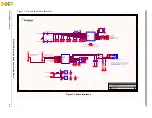
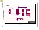
-CS0 to enable the Flash ROM (See
.”)
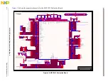
-SDRAS, -SDCAS, and -SDRAM_CS1 to enable the SDRAM (See
The chip select mechanism of the MCF5251 processor allows the memory mapping to be defined for the
required memory space (User/Supervisor, Program/Data spaces).
All of the MCF5251 internal registers, configuration registers, parallel I/O port registers, UART registers
and system control registers are mapped by the MBAR registers at any 1- KByte boundary. The MBAR1
register is mapped to 0x10000000 and MBAR2 mapped to 0x80000000 by the dBUG monitor. For a
complete map of these registers, see the
MCF5251 Reference Manual
.
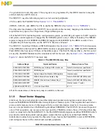
The M5251C3 board has 8 Mbytes of SDRAM installed. See
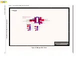
of the SDRAM on the board. The dBUG ROM monitor is programmed in one AMD Am29LV160DB-90
Flash ROM, which occupies 2 Mbytes of the address space. The first 256 Kbytes (that is., the first sector)
are used by the ROM Monitor and the remainder is left for the user. (See
shows the M5251C3 memory map.
All of the unused area of the memory map is available to the user.
3.1.9
Reset Vector Mapping
After reset, the processor attempts to read the initial stack pointer and program counter values from
locations $00000000 & $00000004 (the first eight bytes of memory space). This requires the board to have
a non-volatile memory device in this range with the correct information stored in it. In some systems,
however, it is preferred to have RAM starting at address $00000000. The MCF5251 processor chip-select
zero (-CS0) responds to any accesses after reset until the CSMR0 is written. Since -CS0 (the global chip
select) is connected to the Flash ROM (U11), the Flash ROM initially appears at address $00000000 which
provides the initial stack pointer and program counter (the first eight bytes of the Flash ROM). The
initialization routine then programs the chip-select logic, locates the Flash ROM to start at $FFE00000,
and configures the rest of the internal and external peripherals.
Table 3-1 The M5272C3 Memory Map
Address Range
Signal and Device
Memory Access Time
$00000000-$00020000
SDRAM space for dBug ROM monitor use
Refer to manufacturer specification
$00020000-$003FFFFF
SDRAM space
Refer to manufacturer specification
$10000000-$100003FF
System Integration Module (SIM) registers
Internal access
$10000000-$10000054
MBAR - Module Base Address Reg.
Refer to MCF5251UM SIM section
$80000000-$80000198
MBAR2 - Module Base Address Reg. 2
Refer to MCF5251UM SIM section
$20000000-$20000FFF
SRAM
Internal access (1 cycle)
$FFE00000-$FFFFFFFF
-CS0, 2M Flash ROM
8-7-7-7
Содержание freescale M5251C3
Страница 1: ...Document Number M5251C3UG Rev 0 05 2006 M5251C3 Evaluation Board Users Guide ...
Страница 6: ...M5251C3 Evaluation Board Users Guide Rev 0 vi Freescale Semiconductor ...
Страница 14: ...M5251C3 Evaluation Board Users Guide Rev 0 1 8 Freescale Semiconductor Figure 1 4 Default Jumper Locations ...
Страница 18: ...M5251C3 Evaluation Board Users Guide Rev 0 1 12 Freescale Semiconductor ...
Страница 42: ...M5251C3 Evaluation Board Users Guide Rev 0 2 24 Freescale Semiconductor ...
Страница 68: ...M5251C3 Evaluation Board Users Guide Rev 0 B 6 Freescale Semiconductor ...