


M5251C3 Evaluation Board Users Guide, Rev. 0
Freescale Semiconductor
3-1
Chapter 3
Hardware Description and Reconfiguration
This chapter provides a functional description of the M5251C3 board hardware. With the description given
here and the schematic diagrams in Appendix A, the user can gain a good understanding of the board's
design. In this manual, an active low signal is indicated by a "-" preceding the signal name in the text and
a bar over the signal name in the schematics.
3.1
Processor and Support Logic
This part of the chapter discusses the CPU and general support logic on the M5251C3 board.
3.1.1
Processor
The microprocessor used on the M5251C3 is the highly integrated ColdFire® MCF5251, 32-bit processor.
The MCF5251 implements a ColdFire Version 2 core with 8-Kbyte instruction cache, three UART
channels, two timers, 128-Kbytes of SRAM, a QSPI (Queued Serial Peripheral Interface) module, two I
2
C
modules, 3x I
2
S modules, an IDE module, a dedicate ATA interface with DMA support, two FlexCAN
modules, an OTG USB 2.0 controller with integrated physical interface, Real Time Clock (RTC), a Flash
memory stick interface, 60 parallel I/O ports (which are multiplexed with other signals) and the system
integration module (SIM). All of the core processor registers are 32 bits wide except for the Status Register
(SR) which is 16 bits wide. This processor communicates with external devices over a 16-bit wide data
bus, D[31:16]. The chip can address 64 Mbytes of memory space using a 25-bit wide address bus and
internal chip-select logic.
The MCF5251 processor has the capability to support both an IEEE JTAG-compatible port and a BDM
debug port. These ports are multiplexed and can be used with third party tools to allow the user to
download code to the board. The board is configured to boot up in the normal/BDM mode of operation.
The BDM signals are available at port (J12). The processor also has the logic to generate up to four (4)
chip selects, and support for a bank of SDRAM (included on the evaluation board as 8 Mbytes in total
configured as 4 M x 16). The -SDRAM_CS1 signal is used to provide selection and control of this bank
of SDRAM.
3.1.2
Reset Logic
The reset logic provides system initialization. Reset occurs during power-on or via assertion of the signal
-RESET which causes the MCF5251 to reset. Reset is also triggered by the reset switch (S1) which resets
the entire processor/system.
A hard reset and voltage sense controller (U18) is used to produce an active low power-on RESET signal.
The reset switch S1 is fed into U18 which generates the signal which is fed to the MCF5251 reset, -RESET.
The -RESET signal is an open collector signal and so can be wire OR’ed with other reset signals from
additional peripherals.
dBUG configures the MCF5251 microprocessor internal resources during initialization. The instruction
cache is invalidated and disabled. The Vector Base Register, VBR, contains an address which initially
Содержание freescale M5251C3
Страница 1: ...Document Number M5251C3UG Rev 0 05 2006 M5251C3 Evaluation Board Users Guide ...
Страница 6: ...M5251C3 Evaluation Board Users Guide Rev 0 vi Freescale Semiconductor ...
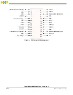
Страница 14: ...M5251C3 Evaluation Board Users Guide Rev 0 1 8 Freescale Semiconductor Figure 1 4 Default Jumper Locations ...
Страница 18: ...M5251C3 Evaluation Board Users Guide Rev 0 1 12 Freescale Semiconductor ...
Страница 42: ...M5251C3 Evaluation Board Users Guide Rev 0 2 24 Freescale Semiconductor ...
Страница 68: ...M5251C3 Evaluation Board Users Guide Rev 0 B 6 Freescale Semiconductor ...