


NXP Semiconductors
KTFRDMHB2001FEVMUG
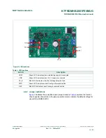
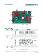
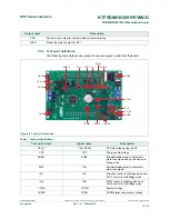
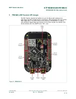
FRDM-HB2001FEVM evaluation board
KTFRDMHB2001FEVMUG
All information provided in this document is subject to legal disclaimers.
© NXP B.V. 2016. All rights reserved
User guide
Rev. 1.0 — 25 May 2016
18 / 35
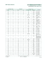
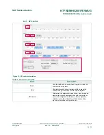
FRDM-HB2001FEVM
FRDM-KL25Z
Pin hardware name
Header
Pin
Header
Pin
FRDM-HB2001FEVM
FRDM-KL25Z
Description
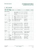
J24
13
J1
13
N/C
PTC10
Not Connected
J24
14
J1
14
N/C
PTC8
No Connection
J24
15
J1
15
N/C
PTC11
Not Connected
J24
16
J1
16
N/C
PTC9
No Connection
J10
1
J2
1
DATA0/IN1
PTC12
IN1 signal for the H-
Bridge
J10
2
J2
2
N/C
PTA13
No Connection
J10
3
J2
3
DATA1/IN2
PTC13
IN2 signal for the H-
Bridge
J10
4
J2
4
N/C
PTD5
No Connection
J10
5
J2
5
FS_B
PTC16
Fault status pin to
report fault
J10
6
J2
6
CS_B
PTD0
Chip select bar pin
J10
7
J2
7
N/C
PTC17
No Connection
J10
8
J2
8
MOSI
PTD2
Master output serial
input
J10
9
J2
9
N/C
PTA16
No Connection
J10
10
J2
10
MISO
PTD3
Master input serial
output
J10
11
J2
11
N/C
PTA17
No Connection
J10
12
J2
12
SCLK
PTD1
Clock for SPI
J10
13
J2
13
N/C
PTE31
No Connection
J10
14
J2
14
GND
GND
No Connection
J10
15
J2
15
N/C
N/C
No Connection
J10
16
J2
16
N/C
VREFH
No Connection
J10
17
J2
17
CFB_READ
PTD6
ADC input for
monitoring the CFB
pin
J10
18
J2
18
N/C
PTE0
Disable signal to tri-
state the output and
put the part in Sleep
mode (Active Low)
J10
19
J2
19
N/C
PTD7
No Connection
J10
20
J2
20
FRDM_VDD
PTE1
No Connection
J23
1
J10
1
N/C
PTE20
No Connection
J23
2
J10
2
N/C
PTB0
No Connection
J23
3
J10
3
N/C
PTE21
No Connection
J23
4
J10
4
N/C
PTB1
No Connection
J23
5
J10
5
N/C
PTE22
No Connection
J23
6
J10
6
N/C
PTB2
No Connection
J23
7
J10
7
N/C
PTE23
No Connection
J23
8
J10
8
N/C
PTB3
No Connection
J23
9
J10
9
N/C
PTE29
No Connection
J23
10
J10
10
N/C
PTC2
No Connection
J23
11
J10
11
N/C
PTE30
No Connection
J23
12
J10
12
N/C
PTC1
No Connection
J25
1
J9
1
N/C
PTB8
No Connection
J25
2
J9
2
N/C
SDA_PTD5
No Connection
J25
3
J9
3
N/C
PTB9
No Connection