


NXP Semiconductors
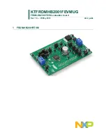
KTFRDMHB2001FEVMUG
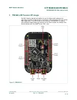
FRDM-HB2001FEVM evaluation board
KTFRDMHB2001FEVMUG
All information provided in this document is subject to legal disclaimers.
© NXP B.V. 2016. All rights reserved
User guide
Rev. 1.0 — 25 May 2016
11 / 35
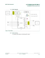
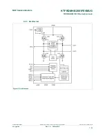
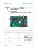
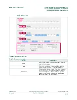
DIS
VDD
CFB
ENBL
IN2
IN1
EX_IN
CFB_R
VDD_REG
MOSI
SCLK
MISO
CS_B
VDDQ
FS_B
Figure 7. Jumper definitions
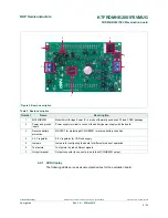
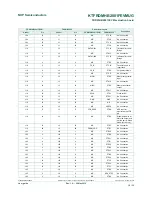
Table 4. Jumper locations
Name
Signal
Jumper
position
Connection
1−2
IN1 control through MCU parallel output on J10 Pin 1 (DATA0)
J1
IN1
2−3
IN1 control through MCU parallel output on J10 Pin 1 (DATA0)
1−2
DIS control through MCU parallel output on J10 Pin 13 (CTRL1)
J2
DIS
2−3
DIS connected to GND to keep the outputs enabled
1−2
IN2 control through MCU parallel output on J10 Pin 3 (DATA1)
J3
IN2
2−3
IN2 control through external input on J15 Pin 2
1−2
CS_B control through MCU SPI output J10 Pin 6 (SPI_CS_B)
J4
CS_B
2−3
CS_B pulled up to VDD for operation without SPI
1−2
ENBL control through MCU parallel output J10 Pin 11 (CTRL0)
J5
ENBL
2−3
ENBL pulled up to VDD to keep the outputs enabled
1−2
SPI clock SCLK from MCU J10 Pin 12 (SPI_SCLK)
J6
SCLK
2−3
SCLK connected to GND for operation without SPI
1−2
MOSI control through MCU SPI output J10 Pin 8 (SPI_MOSI)
J7
MOSI
2−3
MOSI connected to GND for operation without SPI
1−2
MISO control through MCU SPI output J10 Pin 10 (SPI_MISO)
J8
MISO
2−3
MISO not connected for operation without SPI
J11
CFB
1−2
CFB connected to 200 Ω resistor