


NXP Semiconductors
KTFRDMHB2001FEVMUG
FRDM-HB2001FEVM evaluation board
KTFRDMHB2001FEVMUG
All information provided in this document is subject to legal disclaimers.
© NXP B.V. 2016. All rights reserved
User guide
Rev. 1.0 — 25 May 2016
14 / 35
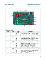
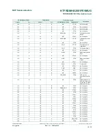
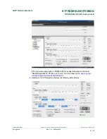
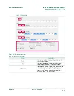
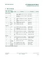
Test point name
Signal name
Description
FSB1
FSB
Fault status monitoring pin
VDD1
VDD
V
DD
supply for the part
CS_B1
CS_B
Chip select bar
SCLK1
SCLK
Clock for SPI
MOSI1
MOSI
Master output slave input signal
MISO1
MISO
Master input slave output signal
GND
GND
Ground signal
GND1
GND
Ground signal
GND2
GND
Ground signal
GND3
GND
Ground signal
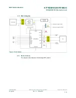
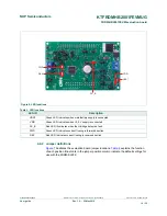
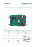
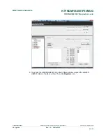
4.4.6 Screw terminal connections
The board has the following screw terminal connections to connect the power supply and
the load.
J21
J20
Figure 9. Screw terminal locations
Table 8. Screw terminal connections
Screw
terminal name
Description
J20
Power supply connector for the MC33HB2001
J21
Output connector to connect load