


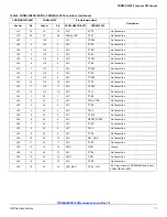


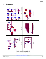


Schematic
FRDM-HB2001-EVM evaluation board
, Rev. 1.0
NXP Semiconductors
25
6
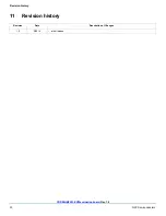
Schematic
Figure 21. Evaluation Board Schematic
Power Supply
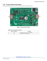
Jumpers
Main Circuit
Main Signal
Test
Points
SPI Signal Test Points
Outputs
SPI Connector
IN1 (Option for
input with and
without SPI)
IN2 (Option for
input with and
without SPI)
ENBL (Option for
input with and
without SPI)
DIS (Option for
input with and
without SPI)
CS_B (Option for
input with and
without SPI)
SCLK (Option for
input with and
without SPI)
MOSI (Option for
input with and
without SPI)
MISO (Option for
input with and
without SPI)
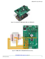
IN1 and IN2
External Inputs
VDDQ Supply
from the
regulator
Current Feedback
Do not populate
FRDM_VDD
provides 3.3V
instead of 5V
All settings jumper position
1-2 for operation with MCU and
2-3 for manual operation.
Jumper setting 1-2 for VDD
through regulator and 2-3
for VDD supply through
FRDM board.
VPWR
CCP
OUT2
ENBL
DIS
IN2
IN1
CS_B
SCLK
MOSI
MISO
GND
VDD
Q
CCP
ENBL
IN2
IN1
VPWR
VDDQ
GND
GND
GND
GND
CS_B
SCLK
MOSI
MISO
OUT1
VBATT
CCP
VPWR
VDD
FS_B
FS_B
VPWR
VDD_REG
VDD
DATA0
IN1
EX_IN1
SPI_CS_B
SPI_MOSI
SPI_MISO
SPI_SCLK
DATA1
IN2
EX_IN2
CTRL0
ENBL
DATA0
DATA1
CTRL0
CTRL1
CTRL1
DIS
VDD
CS_B
SPI_CS_B
SPI_SCLK
SCLK
SPI_MOSI
MOSI
SPI_MISO
MISO
VDD
CFB
OUT1
OUT2
VDD
VDDQ
EX_IN1
EX_IN2
CFB_READ
FRDM_VDD
VDD
FRDM_VDD
CFB_READ
CFB
DIS
VDD_REG
CCP
CFB_READ
FS_B
R2
47K
J25
HDR_2X8
1
2
3
4
6
5
7
8
9
10
11
12
13
14
15
16
FWD
GREEN
A
C
FS_B_
HDR_1X2
1
2
J20
CON 1X2 TB TH
1
2
R204
1K
CCP
R1
1M
DIS
HDR_1X3
1
2
3
C5
0.033UF
IN_1
CFB_R
HDR_1X2
1
2
VDD1
MISO
HDR_1X3
1
2
3
VDD_
HDR_1X3
1
2
3
J24
HDR_2X8
1
2
3
4
6
5
7
8
9
10
11
12
13
14
15
16
R206
4.70K
CFB
HDR_1X2
1
2
VDDQ
HDR_1X3
1
2
3
CFB_V
0
IN2
HDR_1X3
1
2
3
R210
0
EX_IN
HDR_1X2
1
2
U1
MC33HB200EKAF
AG
ND1
1
ENBL
2
DIS
3
IN2
4
IN1
5
CFB
6
FS
7
VPWR1
8
VPWR2
9
OUT1_10
10
OUT1_11
11
NC_12
12
NC_13
13
NC_14
14
PGN
D1
15
PGN
D2
16
PGN
D3
17
PGN
D4
18
AG
ND2
19
NC_20
20
NC_21
21
OUT2_22
22
OUT2_23
23
VPWR3
24
VPWR4
25
CCP
26
CS
27
VDDQ
28
MISO
29
SCLK
30
MOSI
31
DGND
32
EP
33
OUT
CON 1X2 TB TH
1
2
REV
RED
A
C
IN_2
D57
BAS70TW-7-F
2
1
3
4
5
6
C8
0.1uF
R207
4.70K
C4
0.033UF
MISO1
J23
HDR_2X6
1
2
3
4
6
5
7
8
9
10
11
12
C3
0.1 UF
VBAT
GREEN
A
C
VDD
GREEN
A
C
CS_B
HDR_1X3
1
2
3
VDDQ1
D59
SMBJ40
A
C
FS_B1
Q3
SMMBTA06LT1G
2
3
1
GND
R188
0
DIS1
R193
0
R10
10K
R202
200
Q1
IPD30N06S2-15
1
3
4
MOSI1
GND1
J10
HDR_10X2
1
2
3
4
6
5
7
8
9
10
11
12
13
14
15
16
17
18
19
20
ENBL
HDR_1X3
1
2
3
+
C2
100UF
GND2
R203
1K
R208
4.70K
VPWR
U2
MC7805ABD2TG
OUT
3
IN
1
GND
4
R187
0
GND3
R209
4.70K
D58
1N4148WS
A
C
SCLK1
VDD_REG
HDR_1X2
1
2
ENBL1
SCLK
HDR_1X3
1
2
3
C1
0.1 UF
C9
0.047UF
C7
0.33UF
FS_B
RED
A
C
IN1
HDR_1X3
1
2
3
CS_B1
MOSI
HDR_1X3
1
2
3