


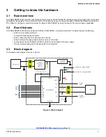


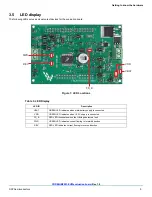


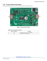


Getting to know the hardware
FRDM-HB2001-EVM evaluation board
, Rev. 1.0
12
NXP Semiconductors
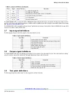
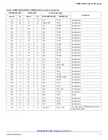
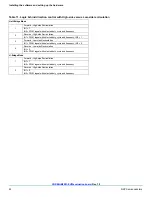
Figure 9. Test point locations
Table 7. Test point definitions
Test Point Name
Signal Name
Description
CFB_V
CFB_READ
CFB pin voltage going to ADC
CCP
CCP
Charge pump voltage
ENBL1
ENBL
Enable/Disable signal to activate/tri-state the outputs and put the device to Sleep mode
DIS1
DIS
Enable/Disable signal to activate/tri-state the outputs
IN_1
IN1
Direction control in H-Bridge mode and OUT1 control in Half-Bridge mode
IN_2
IN2
PWM control in H-Bridge mode and OUT2 control in Half-Bridge mode
VPWR
VPWR
System voltage
VDDQ1
VDDQ
VDDQ Digital output supply voltage
FSB1
FSB
Fault status monitoring pin
VDD1
VDD
V
DD
supply for the part
CS_B1
CS_B
Chip select bar
SCLK1
SCLK
Clock for SPI
MOSI1
MOSI
Master output slave input signal
MISO1
MISO
Master input slave output signal
GND
GND
Ground signal
GND1
GND
Ground signal
GND2
GND
Ground signal
GND3
GND
Ground signal
GND1
ENBL1
CCP
MISO1
CFB_V
VDD1
GND
IN_2
DIS1 IN_1
FS_B1
MOSI1
VPWR
SCLK1
GND2
CS_B1
GND3
VDDQ1