Nvis 5586A
Nvis Technologies Pvt. Ltd.
22
Maximum Mode 8086 System
Here the only difference between in timing diagram between minimum mode and maximum
mode is the status signals used and the available control and advanced command signals. R0,
S1*, S2* are set at the beginning of bus cycle. 8288 bus controller will output a pulse as on
the ALE and apply a required signal to its DT / R* pin during T1. In T2, 8288 will set
DEN=1 thus enabling transceivers, and for an input it will activate MRDC* or IORC*. These
signals are activated until T4. For an output, the AMWC* or AIOWC* is activated from T2
to T4 and MWTC* or IOWC* is activated from T3 to T4. The status bit S0* to S2* remains
active until T3 and become passive during T3 and T4
.
If reader input is not activated before
T3, wait state will be inserted between T3 and T4.
Timings for RQ/ GT* Signals:
The request/grant response sequence contains a series of
three pulses. The request/grant pins are checked at each rising pulse of clock input. When a
request is detected and if the conditions for HOLD request are satisfied, the processor issues
a grant pulse over the RQ/GT* pin immediately during T4 (current) or T1 (next) state. When
the requesting master receives this pulse, it accepts the control of the bus; it sends a release
pulse to the processor using RQ/GT* pin.
Содержание 5586A
Страница 2: ...Nvis 5586A Nvis Technologies Pvt Ltd 2...
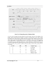
Страница 23: ...Nvis 5586A Nvis Technologies Pvt Ltd 23 Memory Read Timing in Maximum Mode...
Страница 30: ...Nvis 5586A Nvis Technologies Pvt Ltd 30...
Страница 48: ...Nvis 5586A Nvis Technologies Pvt Ltd 48 Diagram of module RESET power Instruction Set Note...
Страница 170: ...Nvis 5586A Nvis Technologies Pvt Ltd 170...

