Nvis 5586A
Nvis Technologies Pvt. Ltd.
13
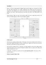
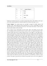
Status line S5 reflects the status of another internal characteristic of the 8086. It is the logic
level of the internal enable flag. The last status bit S6 is always at the logic 0 level.
Control Signals:
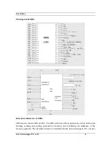
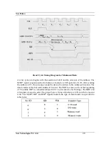
The control signals are provided to support the 8086 memory I/O
interfaces. They control functions such as when the bus is to carry a valid address in which
direction data are to be transferred over the bus, when valid write data are on the bus and
when to put read data on the system bus.
ALE is a pulse to logic 1 that signals external circuitry when a valid address word is on the
bus. This address must be latched in external circuitry on the 1-to-0 edge of the pulse at ALE.
Another control signal that is produced during the bus cycle is BHE i.e. bank high enable.
Logic 0 on this used as a memory enable signal for the most significant byte half of the data
bus D8 through D1. These lines also serve a second function, which is as the S7 status line.
Using the M/IO* and DT/R* lines, the 8086 signals which type of bus cycle is in progress
and in which direction data are to be transferred over the bus. The logic level of M/IO* tells
external circuitry whether a memory or I/O transfer is taking place over the bus. Logic 1 at
this output signals a memory operation and logic 0 an I/O operation. The direction of data
transfer over the bus is signaled by the logic level output at DT/R*. When this line is logic 1
during the data transfer part of a bus cycle, the bus is in the transmit mode. Therefore, data
are either written into memory or output to an I/O device. On the other hand, logic 0 at
DT/R* signals that the bus is in the receive mode. This corresponds to reading data from
memory or input of data from an input port. The signals read RD and write WR indicate that
a read bus cycle or a write bus cycle is in progress. The 8086 switches WR to logic 0 to
intimate external device about valid write or output data are on the bus. On the other hand,
RD indicates that the 8086 is performing a read of data of the bus. During read operations,
one other control signal is also supplied. This is DEN (data enable) and it signals external
devices when they should put data on the bus. There is one other control signal that is
involved with the memory and I/O interface. This is the READY signal. READY signal is
used to insert wait states into the bus cycle such that it is extended by a number of clock
periods. This signal is provided by an external clock generator device and can be supplied by
Содержание 5586A
Страница 2: ...Nvis 5586A Nvis Technologies Pvt Ltd 2...
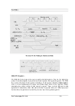
Страница 23: ...Nvis 5586A Nvis Technologies Pvt Ltd 23 Memory Read Timing in Maximum Mode...
Страница 30: ...Nvis 5586A Nvis Technologies Pvt Ltd 30...
Страница 48: ...Nvis 5586A Nvis Technologies Pvt Ltd 48 Diagram of module RESET power Instruction Set Note...
Страница 170: ...Nvis 5586A Nvis Technologies Pvt Ltd 170...


