background image

CHAPTER  1   GENERAL  (

µ

PD789860  SUBSERIES) 

User’s Manual  U14826EJ5V0UD 

23

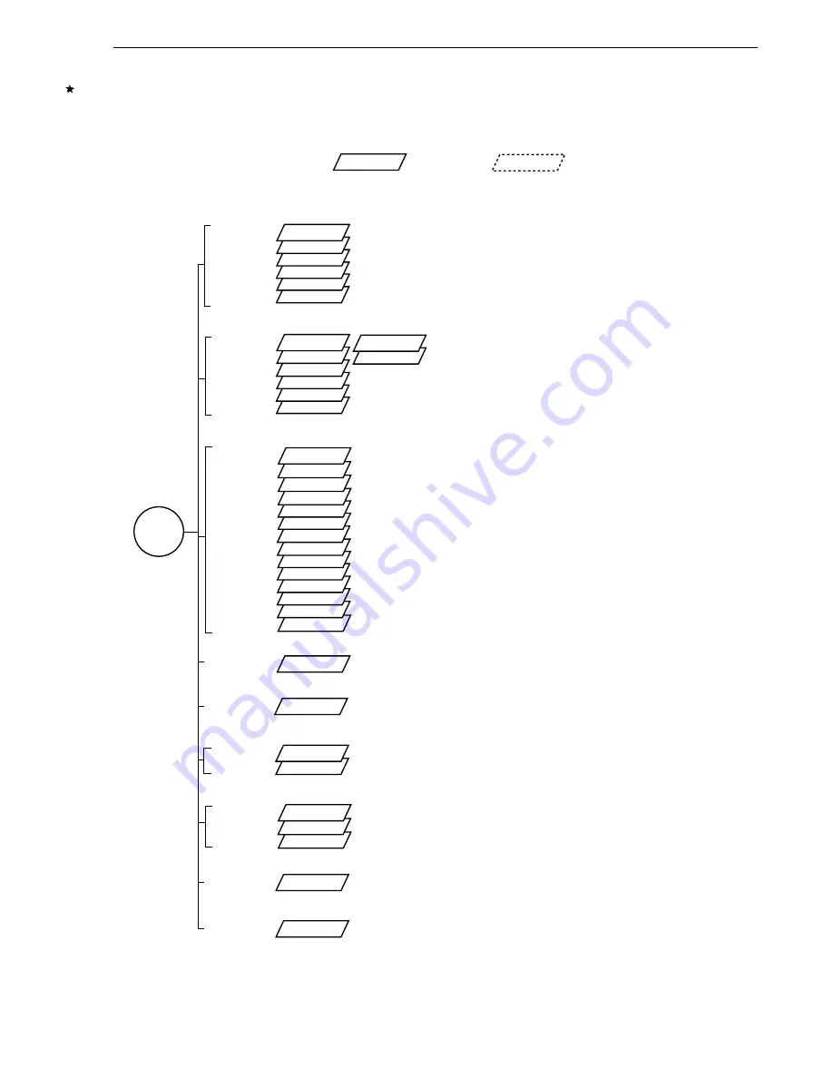
1.6  78K/0S Series Lineup 

The products in the 78K/0S Series are listed below.  The names enclosed in boxes are subseries names. 
 

Products under 
development

Products in mass 
production

Y subseries supports SMB.

52-pin

SIO +  resistance division method LCD (24 

×

 4)

8-bit A/D + internal voltage boosting method LCD (23 

×

 4)

PD789327

LCD drive

80-pin

80-pin

PD789436

PD789446

PD789426

PD789456

PD789417A

PD789407A

PD789316

PD789467

PD789306

PD789426 with 10-bit A/D

PD789446 with 10-bit A/D

SIO + 8-bit A/D + resistance division method LCD (28 

×

 4)

SIO + 8-bit A/D + internal voltage boosting method LCD (15 

×

 4)

PD789407A with 10-bit A/D

SIO + 8-bit A/D + internal voltage boosting method LCD (5 

×

 4)

RC oscillation version of    PD789306

SIO + internal voltage boosting method LCD (24 

×

 4)

64-pin

64-pin

52-pin

64-pin

64-pin

64-pin

SIO + 10-bit A/D + internal voltage boosting method LCD (28 

× 

4)

80-pin

SIO + 8-bit A/D + resistance division method LCD (28 

×

 4)

80-pin

PD789479

PD789489

64-pin

Small-scale package, general-purpose applications

78K/0S 
Series

On-chip UART and capable of low-voltage (1.8 V) operation

PD789074 with subsystem clock added

Inverter control

44-pin

PD789842

On-chip inverter controller and UART

44-pin

Small-scale package, general-purpose applications and A/D function

44-pin

PD789167 with 10-bit A/D 

PD789104A with enhanced timer

PD789177Y

PD789167Y

USB

88-pin

PD789830

PD789835

144-pin

UART + dot LCD (40 

×

 16)

UART + 8-bit A/D + dot LCD (total display outputs: 96)

42-/44-pin

44-pin

30-pin

20-pin

20-pin

PD789026 with enhanced timer function

RC oscillation version of    PD789052

VFD drive

52-pin

64-pin

PD789871

On-chip VFD controller (total display outputs: 25)

Meter control

PD789881

UART + resistance division method LCD (26 

×

 4)

30-pin

PD789074 with enhanced timer function and expanded ROM and RAM

44-pin

PD789800

For PC keyboard.  On-chip USB function

Keyless entry

20-pin

20-pin

30-pin

On-chip POC and key return circuit

RC oscillation version of    PD789860

On-chip bus controller

On-chip CAN controller

µ
µ

µ

PD789074

PD789088

PD789062

PD789046

PD789026

PD789052

µ
µ

µ

µ

µ

µ

µ

µ

µ

µ

PD789860

PD789861

PD789862

µ

µ

µ

µ

µ

µ

µ

µ

µ

µ

µ

µ

µ

µ

µ

30-pin

PD789850A

µ

µ

µ

µ

µ

µ

PD789860 without EEPROM, POC, and LVI

µ

µ

µ

µ

30-pin

30-pin
30-pin

30-pin

PD789124A

PD789134A

PD789104A

PD789114A

PD789124A with 10-bit A/D

RC oscillation version of    PD789104A

PD789104A with 10-bit A/D
PD789026 with 8-bit A/D and multiplier added

µ

µ

µ
µ

µ

µ

µ

µ

µ

µ

µ

PD789860 with enhanced timer function, SIO, and expanded ROM and RAM

µ

µ

µ

PD789167

PD789177

µ

44-pin

PD789852

µ

PD789850A with enhanced timer and A/D converter, etc.

µ

µ


Remark

  VFD (Vacuum Fluorescent Display) is referred to as FIP

TM

 (Fluorescent Indicator Panel) in some 

documents, but the functions of the two are the same.  

Содержание PD789860

Страница 1: ...PD789860 µPD78E9860A µPD789861 µPD78E9861A µPD789860 A µPD789860 789861 Subseries 8 Bit Single Chip Microcontrollers Printed in Japan Document No U14826EJ5V0UD00 5th edition Date Published June 2004 NS CP K 2000 2003 ...

Страница 2: ...User s Manual U14826EJ5V0UD 2 MEMO ...

Страница 3: ...ssible and quickly dissipate it when it has occurred Environmental control must be adequate When it is dry a humidifier should be used It is recommended to avoid using insulators that easily build up static electricity Semiconductor devices must be stored and transported in an anti static container static shielding bag or conductive material All test and measurement tools including work benches an...

Страница 4: ...ety of NEC Electronics products customers agree and acknowledge that the possibility of defects thereof cannot be eliminated entirely To minimize risks of damage to property or injury including death to persons arising from defects in NEC Electronics products customers must incorporate sufficient safety measures in their design such as redundancy fire containment and anti failure features NEC Elec...

Страница 5: ...anch Seoul Korea Tel 02 558 3737 NEC Electronics Shanghai Ltd Shanghai P R China Tel 021 5888 5400 NEC Electronics Taiwan Ltd Taipei Taiwan Tel 02 2719 2377 NEC Electronics Singapore Pte Ltd Novena Square Singapore Tel 6253 8311 J04 1 NEC Electronics Europe GmbH Duesseldorf Germany Tel 0211 65030 Sucursal en España Madrid Spain Tel 091 504 27 87 Vélizy Villacoublay France Tel 01 30 67 58 00 Succur...

Страница 6: ... 4 Notes for EEPROM Writing p 86 CHAPTER 9 8 BIT TIMERS 30 AND 40 Addition of description output to EEPROM to Figure 9 2 Block Diagram of Timer 40 pp 140 142 CHAPTER 14 INTERRUPT FUNCTIONS Modification of caution in Figure 14 3 Format of Interrupt Mask Flag Register 0 Modification of a signal name in Figure 14 6 Timing of Non Maskable Interrupt Request Acknowledgment pp 151 152 154 155 CHAPTER 15 ...

Страница 7: ...ation µPD789860 Subseries is described as fX and the system clock oscillation frequency of the RC oscillation µPD789861 Subseries is described as fCC Purpose This manual is intended to give users on understanding of the functions described in the Organization below Organization Two manuals are available for the µPD789860 789861 Subseries this manual and the Instruction Manual common to the 78K 0S ...

Страница 8: ...The name of a bit whose number is enclosed with is reserved in the assembler and is defined as an sfr variable by the pragma sfr directive for the C compiler To learn the detailed functions of a register whose register name is known See APPENDIX C REGISTER INDEX To learn the details of the instruction functions of the 78K 0S Series Refer to 78K 0S Series Instructions User s Manual U11047E separate...

Страница 9: ...ts Related to Development Hardware Tools User s Manuals Document Name Document No IE 78K0S NS In Circuit Emulator U13549E IE 78K0S NS A In Circuit Emulator U15207E IE 789860 NS EM1 Emulation Board U16499E Documents Related to EEPROM Program Memory Writing Document Name Document No PG FP3 Flash Memory Programmer User s Manual U13502E PG FP4 Flash Memory Programmer User s Manual U15260E Other Relate...

Страница 10: ...n Top View 29 2 5 78K 0S Series Lineup 30 2 6 Block Diagram 33 2 7 Overview of Functions 34 CHAPTER 3 PIN FUNCTIONS 35 3 1 Pin Function List 35 3 2 Description of Pin Functions 36 3 2 1 P00 to P07 Port 0 36 3 2 2 P20 P21 Port 2 36 3 2 3 P40 to P43 Port 4 36 3 2 4 RESET 36 3 2 5 X1 X2 µPD789860 Subseries 36 3 2 6 CL1 CL2 µPD789861 Subseries 36 3 2 7 VDD 37 3 2 8 VSS 37 3 2 9 VPP µPD78E9860A 78E9861...

Страница 11: ...ressing 57 4 4 7 Stack addressing 57 CHAPTER 5 EEPROM DATA MEMORY 58 5 1 Memory Space 58 5 2 EEPROM Configuration 58 5 3 EEPROM Control Register 58 5 4 Notes for EEPROM Writing 61 CHAPTER 6 PORT FUNCTIONS 63 6 1 Port Functions 63 6 2 Port Configuration 63 6 2 1 Port 0 64 6 2 2 Port 2 65 6 2 3 Port 4 66 6 3 Port Function Control Registers 67 6 4 Operation of Port Functions 68 6 4 1 Writing to I O p...

Страница 12: ... Timers 30 40 Configuration 84 9 3 8 Bit Timers 30 40 Control Registers 88 9 4 8 Bit Timers 30 40 Operation 93 9 4 1 Operation as 8 bit timer counter 93 9 4 2 Operation as 16 bit timer counter 102 9 4 3 Operation as carrier generator 109 9 4 4 Operation as PWM output timer 40 only 114 9 5 Notes on Using 8 Bit Timers 30 40 116 CHAPTER 10 WATCHDOG TIMER 118 10 1 Watchdog Timer Functions 118 10 2 Wat...

Страница 13: ...operation 141 14 4 2 Maskable interrupt request acknowledgment operation 143 14 4 3 Multiple interrupt servicing 146 14 4 4 Interrupt request pending 147 CHAPTER 15 STANDBY FUNCTION 148 15 1 Standby Function and Configuration 148 15 1 1 Standby function 148 15 1 2 Standby function control register 149 15 2 Standby Function Operation 150 15 2 1 HALT mode 150 15 2 2 STOP mode 153 CHAPTER 16 RESET FU...

Страница 14: ...G 196 CHAPTER 23 RECOMMENDED SOLDERING CONDITIONS 197 APPENDIX A DEVELOPMENT TOOLS 199 A 1 Software Package 201 A 2 Language Processing Software 201 A 3 Control Software 202 A 4 EEPROM Program Memory Writing Tools 202 A 5 Debugging Tools Hardware 203 A 6 Debugging Tools Software 204 APPENDIX B NOTES ON TARGET SYSTEM DESIGN 205 APPENDIX C REGISTER INDEX 206 C 1 Register Name Index in Alphabetical O...

Страница 15: ...l Register 10 59 6 1 Block Diagram of P00 to P07 64 6 2 Block Diagram of P20 65 6 3 Block Diagram of P21 66 6 4 Block Diagram of P40 to P43 66 6 5 Format of Port Mode Register 67 7 1 Block Diagram of Clock Generator 69 7 2 Format of Processor Clock Control Register 70 7 3 External Circuit of System Clock Oscillator 71 7 4 Examples of Incorrect Resonator Connection 72 7 5 Switching Between System C...

Страница 16: ...rnal Event Counter Operation with 16 Bit Resolution 106 9 18 Timing of Square Wave Output with 16 Bit Resolution 108 9 19 Timing of Carrier Generator Operation When CR40 N CRH40 M M N 111 9 20 Timing of Carrier Generator Operation When CR40 N CRH40 M M N 112 9 21 Timing of Carrier Generator Operation When CR40 CRH40 N 113 9 22 PWM Output Mode Timing Basic Operation 115 9 23 PWM Output Mode Timing ...

Страница 17: ...ment 142 14 7 Acknowledgment of Non Maskable Interrupt Request 142 14 8 Interrupt Request Acknowledgment Processing Algorithm 144 14 9 Interrupt Request Acknowledgment Timing Example of MOV A r 144 14 10 Interrupt Request Acknowledgment Timing When Interrupt Request Flag Is Set at Last Clock During Instruction Execution 145 14 11 Example of Multiple Interrupts 146 15 1 Format of Oscillation Stabil...

Страница 18: ...nnection Example 164 17 5 Signal Conflict Input Pin of Serial Interface 165 17 6 Abnormal Operation of Other Device 165 17 7 Signal Conflict RESET Pin 166 17 8 Wiring Example for EEPROM Writing Adapter with Pseudo 3 Wire 167 A 1 Development Tools 200 B 1 Connection Condition of Target 205 ...

Страница 19: ...Mode List 83 9 2 Configuration of 8 Bit Timers 30 40 84 9 3 Interval Time of Timer 30 During fX 5 0 MHz Operation 94 9 4 Interval Time of Timer 30 During fCC 1 0 MHz Operation 94 9 5 Interval Time of Timer 40 During fX 5 0 MHz Operation 94 9 6 Interval Time of Timer 40 During fCC 1 0 MHz Operation 94 9 7 Square Wave Output Range of Timer 40 During fX 5 0 MHz Operation 100 9 8 Square Wave Output Ra...

Страница 20: ...Time from Generation of Maskable Interrupt Request to Servicing 143 15 1 Operation Statuses in HALT Mode 150 15 2 Operation After Releasing HALT Mode 152 15 3 Operation Statuses in STOP Mode 153 15 4 Operation After Releasing STOP Mode 155 16 1 Status of Hardware After Reset 158 17 1 Differences Between µPD78E9860A 78E9861A and Mask ROM Versions 159 17 2 Communication Mode List 161 17 3 Pin Connec...

Страница 21: ...s at 5 0 MHz operation with system clock I O ports 14 Timer 3 channels 8 bit timer 2 channels Watchdog timer 1 channel On chip power on clear circuit On chip bit sequential buffer Power supply voltage VDD 1 8 to 5 5 V Operating ambient temperature TA 40 to 85 C 1 2 Applications Keyless entry and other automotive electrical equipment 1 3 Ordering Information Part Number Package Internal ROM µPD7898...

Страница 22: ...commended applications 1 5 Pin Configuration Top View 20 pin plastic SSOP 7 62 mm 300 µPD789860MC 5A4 µPD78E9860AMC 5A4 µPD789860MC A 5A4 RESET X1 X2 VSS IC VPP VDD P00 P01 P02 P03 1 2 3 4 5 6 7 8 9 10 20 19 18 17 16 15 14 13 12 11 P21 TMI P20 TMO BSFO P07 P06 P05 P04 P43 KR13 P42 KR12 P41 KR11 P40 KR10 Caution Connect the IC Internally Connected pin directly to VSS Remark Pin connections in paren...

Страница 23: ... A D function 44 pin PD789167 with 10 bit A D PD789104A with enhanced timer PD789177Y PD789167Y USB 88 pin PD789830 PD789835 144 pin UART dot LCD 40 16 UART 8 bit A D dot LCD total display outputs 96 42 44 pin 44 pin 30 pin 20 pin 20 pin PD789026 with enhanced timer function RC oscillation version of PD789052 VFD drive 52 pin 64 pin PD789871 On chip VFD controller total display outputs 25 Meter co...

Страница 24: ...PD789167 16 K to 24 K 3 ch 1 ch 8 ch 31 µPD789134A 4 ch µPD789124A 4 ch RC oscillation version µPD789114A 4 ch Small scale package general purpose applica tions A D converter µPD789104A 2 K to 8 K 1 ch 1 ch 1ch 4 ch 1 ch UART 1 ch 20 1 8 V µPD789835 24 K to 60 K 6 ch 3 ch 37 1 8 V Note µPD789830 24 K 1 ch 1 ch UART 1 ch 30 2 7 V Dot LCD supported µPD789489 32 K to 48 K 8 ch µPD789479 24 K to 48 K ...

Страница 25: ...1 1 ch 1 ch 8 ch 1 ch UART 1 ch 30 4 0 V µPD789852 24Kto32K 3 ch 8 ch 3 ch UART 2 ch 31 On chip bus controller µPD789850A 16 K 1 ch 1 ch 1 ch 4 ch 2 ch UART 1 ch 18 4 0 V µPD789861 1 8 V RC oscillation version on chip EEPROM µPD789860 4 K 2 ch 1 ch 14 Keyless entry µPD789862 16 K 1 ch 2 ch 1 ch UART 1 ch 22 On chip EEPROM VFD drive µPD789871 4 K to 8 K 3 ch 1 ch 1 ch 1 ch 33 2 7 V Meter control µP...

Страница 26: ...STEM CONTROL RESET X1 X2 PORT 4 P40 P43 78K 0S CPU CORE ROM EEPROM 4 KB 8 bit TIMER EVENT COUNTER40 8 bit TIMER30 CASCADED 16 bit TIMER COUNTER TMO P20 BIT SEQ BUFFER RAM 128 bytes EEPROM 32 bytes KEY RETURN10 KR10 P40 KR13 P43 POWER ON CLEAR POWER ON CLEAR LOW VOLTAGE INDICATOR BSFO P20 Remark Pin connections in parentheses are intended for the µPD78E9860A ...

Страница 27: ...quential buffer 8 bits 8 bits 16 bits Key return function Generates key return signal according to falling edge detection Maskable Internal 5 Vectored interrupt sources Non maskable Internal 1 external 1 Power supply voltage VDD 1 8 to 5 5 V Operating ambient temperature TA 40 to 85 C Package 20 pin plastic SSOP 7 62 mm 300 1 9 Differences Between Standard Quality Grade Products and A Products A m...

Страница 28: ... low speed 8 0 µs at 1 0 MHz operation with system clock I O ports 14 Timer 3 channels 8 bit timer 2 channels Watchdog timer 1 channel On chip power on clear circuit On chip bit sequential buffer Power supply voltage VDD 1 8 to 3 6 V Operating ambient temperature TA 40 to 85 C 2 2 Applications Keyless entry and other automotive electrical equipment 2 3 Ordering Information Part Number Package Inte...

Страница 29: ...P21 TMI P20 TMO BSFO P07 P06 P05 P04 P43 KR13 P42 KR12 P41 KR11 P40 KR10 Caution Connect the IC Internally Connected pin directly to VSS Remark Pin connections in parentheses are intended for the µPD78E9861A BSFO Bit sequential buffer output RESET Reset CL1 CL2 RC oscillator TMI Timer input IC Internally connected TMO Timer output KR10 to KR13 Key return VDD Power supply P00 to P07 Port 0 VPP Prog...

Страница 30: ...d A D function 44 pin PD789167 with 10 bit A D PD789104A with enhanced timer PD789177Y PD789167Y USB 88 pin PD789830 PD789835 144 pin UART dot LCD 40 16 UART 8 bit A D dot LCD total display outputs 96 42 44 pin 44 pin 30 pin 20 pin 20 pin PD789026 with enhanced timer function RC oscillation version of PD789052 VFD drive 52 pin 64 pin PD789871 On chip VFD controller total display outputs 25 Meter c...

Страница 31: ...PD789167 16 K to 24 K 3 ch 1 ch 8 ch 31 µPD789134A 4 ch µPD789124A 4 ch RC oscillation version µPD789114A 4 ch Small scale package general purpose applica tions A D converter µPD789104A 2 K to 8 K 1 ch 1 ch 1ch 4 ch 1 ch UART 1 ch 20 1 8 V µPD789835 24 K to 60 K 6 ch 3 ch 37 1 8 V Note µPD789830 24 K 1 ch 1 ch UART 1 ch 30 2 7 V Dot LCD supported µPD789489 32 K to 48 K 8 ch µPD789479 24 K to 48 K ...

Страница 32: ...1 1 ch 1 ch 8 ch 1 ch UART 1 ch 30 4 0 V µPD789852 24Kto32K 3 ch 8 ch 3 ch UART 2 ch 31 On chip bus controller µPD789850A 16 K 1 ch 1 ch 1 ch 4 ch 2 ch UART 1 ch 18 4 0 V µPD789861 1 8 V RC oscillation version on chip EEPROM µPD789860 4 K 2 ch 1 ch 14 Keyless entry µPD789862 16 K 1 ch 2 ch 1 ch UART 1 ch 22 On chip EEPROM VFD drive µPD789871 4 K to 8 K 3 ch 1 ch 1 ch 1 ch 33 2 7 V Meter control µP...

Страница 33: ...TEM CONTROL RESET CL1 CL2 PORT 4 P40 P43 78K 0S CPU CORE ROM EEPROM 4 KB 8 bit TIMER EVENT COUNTER40 8 bit TIMER30 CASCADED 16 bit TIMER COUNTER TMO P20 BIT SEQ BUFFER RAM 128 bytes EEPROM 32 bytes KEY RETURN10 KR10 P40 KR13 P43 POWER ON CLEAR POWER ON CLEAR LOW VOLTAGE INDICATOR BSFO P20 Remark Pin connections in parentheses are intended for the µPD78E9861A ...

Страница 34: ... 14 CMOS I O 10 CMOS input 4 Timers 8 bit timer 2 channels Watchdog timer 1 channel POC circuit Generates internal reset signal according to comparison of detection voltage to power supply voltage Power on clear circuit LVI circuit Generates interrupt request signal according to comparison of detection voltage to power supply voltage Bit sequential buffer 8 bits 8 bits 16 bits Key return function ...

Страница 35: ...After Reset Alternate Function TMI Input 8 bit timer TM40 input Input P21 TMO Output 8 bit timer TM40 output Input P20 BSFO BSFO Output Bit sequential buffer BSF10 output Input P20 TMO KR10 to KR13 Input Key return input Input P40 to P43 X1 Note 1 Input X2 Note 1 Connecting ceramic crystal resonator for system clock oscillation CL1 Note 2 Input CL2 Note 2 Connecting resistor R and capacitor C for ...

Страница 36: ... sequential buffer b TMI This is the external clock input pin for the timer 40 c TMO This is the output pin of the timer 40 3 2 3 P40 to P43 Port 4 These pins constitute a 4 bit input only port In addition these pins function as the key return input 1 Port mode In port mode P40 to P43 function as a 4 bit input only port For mask ROM versions an on chip pull up resistor can be specified by means of...

Страница 37: ...tion mode by using a jumper on the board If the wiring length between the VPP and VSS pins is too long or if external noise is superimposed on the VPP pin your program may not be executed correctly 3 2 10 IC mask ROM version only The IC Internally Connected pin is used to set the µPD789860 and 789861 to test mode before shipment In normal operation mode directly connect this pin to the VSS pin wit...

Страница 38: ...of Unused Pins P00 to P07 5 P20 TMO BSFO P21 TMI 8 Input Independently connect to VDD or VSS via a resistor Output Leave open P40 KR10 to P43 KR13 mask ROM version 2 E P40 KR10 to P43 KR13 µPD78E9860A 78E9861A Connect directly to VDD RESET 2 I O IC Connect directly to VSS VPP Independently connect to a 10 kΩ pull down resistor or connect directly to VSS Figure 3 1 Pin I O Circuits Schmitt triggere...

Страница 39: ...unction registers SFR 256 8 bits Internal high speed RAM 128 8 bits Reserved Internal ROM 4 096 8 bits Program memory space Data memory space Program area Program area CALLT table area Vector table area Reserved EEPROM data memory 32 8 bits F F F F H 0 F F F H 0 0 8 0 H 0 0 7 F H 0 0 4 0 H 0 0 3 F H 0 0 0 E H 0 0 0 D H 0 0 0 0 H F F 0 0 H F E F F H F E 8 0 H F E 7 F H F 8 2 0 H F 8 1 F H F 8 0 0 H...

Страница 40: ...eserved EEPROM program memory 4 096 8 bits Program memory space Data memory space Program area Program area CALLT table area Vector table area Reserved EEPROM data memory 32 8 bits F F F F H 0 F F F H 0 0 8 0 H 0 0 7 F H 0 0 4 0 H 0 0 3 F H 0 0 0 E H 0 0 0 D H 0 0 0 0 H F F 0 0 H F E F F H F E 8 0 H F E 7 F H F 8 2 0 H F 8 1 F H F 8 0 0 H F 7 F F H 1 0 0 0 H 0 F F F H 0 0 0 0 H ...

Страница 41: ...n branching by RESET input or interrupt request generation Of a 16 bit address the lower 8 bits are stored in an even address and the higher 8 bits are stored in an odd address Table 4 2 Vector Table Vector Table Address Interrupt Request Vector Table Address Interrupt Request 0000H RESET input 0008H INTTM40 0002H INTKR1 000AH INTLVI1 0004H INTWDT 000CH INTEE0 0006H INTTM30 2 CALLT instruction tab...

Страница 42: ... FE80H to FFFFH can be accessed using a unique addressing mode according to its use such as a special function register SFR Figures 4 3 and 4 4 illustrate the data memory addressing Figure 4 3 Data Memory Addressing µPD789860 789861 Special function registers SFR 256 8 bits Internal high speed RAM 128 8 bits Reserved Internal ROM 4 096 8 bits Direct addressing Register indirect addressing Based ad...

Страница 43: ...nternal high speed RAM 128 8 bits Reserved EEPROM program memory 4 096 8 bits Direct addressing Register indirect addressing Based addressing SFR addressing Short direct addressing Reserved EEPROM data memory 32 8 bits F F F F H F F 0 0 H F E F F H F F 2 0 H F E 1 F H F E 8 0 H F E 7 F H F 8 2 0 H F 8 1 F H F 8 0 0 H F 7 F F H 1 0 0 0 H 0 F F F H 0 0 0 0 H ...

Страница 44: ...rogram status word is an 8 bit register consisting of various flags to be set reset by instruction execution Program status word contents are automatically stacked upon interrupt request generation or PUSH PSW instruction execution and are automatically restored upon execution of the RETI and POP PSW instructions RESET input sets PSW to 02H Figure 4 6 Program Status Word Configuration 7 0 IE Z 0 A...

Страница 45: ...e writing saving to the stack memory and is incremented after reading restoring from the stack memory Each stack operation saves restores data as shown in Figures 4 8 and 4 9 Caution Since RESET input makes SP contents undefined be sure to initialize the SP before using the stack Figure 4 8 Data to Be Saved to Stack Memory Interrupt PSW PC15 to PC8 PC15 to PC8 PC7 to PC0 Lower half register pairs ...

Страница 46: ...t registers in pairs can be used as a 16 bit register AX BC DE and HL Registers can be described in terms of function names X A C B E D L H AX BC DE and HL and absolute names R0 to R7 and RP0 to RP3 Figure 4 10 General Purpose Register Configuration a Absolute names R0 15 0 7 0 16 bit processing 8 bit processing RP3 RP2 RP1 RP0 R1 R2 R3 R4 R5 R6 R7 b Function names X 15 0 7 0 16 bit processing 8 b...

Страница 47: ...n operand sfr This manipulation can also be specified with an address 16 bit manipulation Describes a symbol reserved by the assembler for the 16 bit manipulation instruction operand When specifying an address describe an even address Table 4 3 lists the special function registers The meanings of the symbols in this table are as follows Symbol Indicates the addresses of the implemented special fun...

Страница 48: ...are register 40 CR40 FF54H 8 bit compare register H40 CRH40 W Undefined FF55H 8 bit timer counter 40 TM40 R FF56H 8 bit timer mode control register 40 TMC40 R W FF57H Carrier generator output control register 40 TCA40 W FF60H Bit sequential buffer output control register 10 BSFC10 00H FFD8H EEPROM write control register 10 EEWC10 08H FFDDH Power on clear register 1 POCF1 00H Note 2 FFDEH Low volta...

Страница 49: ...Relative addressing Function The value obtained by adding 8 bit immediate data displacement value jdisp8 of an instruction code to the start address of the following instruction is transferred to the program counter PC to branch The displacement value is treated as signed two s complement data 128 to 127 and bit 7 becomes the sign bit In other words the range of branch in relative addressing is be...

Страница 50: ...ow addr High addr 4 3 3 Table indirect addressing Function The table contents branch destination address of the particular location to be addressed by the immediate data of an instruction code from bit 1 to bit 5 are transferred to the program counter PC to branch Table indirect addressing is carried out when the CALLT addr5 instruction is executed This instruction can be used to branch to all the...

Страница 51: ... 4 Register addressing Function The register pair AX contents to be specified with an instruction word are transferred to the program counter PC to branch This function is carried out when the BR AX instruction is executed Illustration 7 0 rp 0 7 A X 15 0 PC 8 7 ...

Страница 52: ...ruction execution 4 4 1 Direct addressing Function The memory indicated by immediate data in an instruction word is directly addressed Operand format Identifier Description addr16 Label or 16 bit immediate data Description example MOV A FE00H When setting addr16 to FE00H Instruction code 0 0 1 0 1 0 0 1 OP Code 0 0 0 0 0 0 0 0 00H 1 1 1 1 1 1 1 0 FEH Illustration 7 0 OP code addr16 low addr16 high...

Страница 53: ...ister of the timer counter are mapped and these SFRs can be manipulated with a small number of bytes and clocks When 8 bit immediate data is at 20H to FFH bit 8 of an effective address is cleared to 0 When it is at 00H to 1FH bit 8 is set to 1 See Illustration below Operand format Identifier Description saddr Label or FE20H to FF1FH immediate data saddrp Label or FE20H to FF1FH immediate data even...

Страница 54: ...n word This addressing is applied to the 256 byte space FF00H to FFFFH However SFRs mapped at FF00H to FF1FH can also be accessed with short direct addressing Operand format Identifier Description sfr Special function register name Description example MOV PM0 A When selecting PM0 for sfr Instruction code 1 1 1 0 0 1 1 1 0 0 1 0 0 0 0 0 Illustration 15 0 SFR Effective address 1 1 1 1 1 1 1 8 7 0 7 ...

Страница 55: ...at is executed When an 8 bit register is specified one of the eight registers is specified with 3 bits in the instruction code Operand format Identifier Description r X A C B E D L H rp AX BC DE HL r and rp can be described with absolute names R0 to R7 and RP0 to RP3 as well as function names X A C B E D L H AX BC DE and HL Description example MOV A C When selecting the C register for r Instructio...

Страница 56: ... accessed is specified with the register pair specify code in the instruction code This addressing can be carried out for all the memory spaces Operand format Identifier Description DE HL Description example MOV A DE When selecting register pair DE Instruction code 0 0 1 0 1 0 1 1 Illustration 15 0 8 D 7 E 0 7 7 0 A DE The contents of addressed memory are transferred Memory address specified by re...

Страница 57: ...paces Operand format Identifier Description HL byte Description example MOV A HL 10H When setting byte to 10H Instruction code 0 0 1 0 1 1 0 1 0 0 0 1 0 0 0 0 4 4 7 Stack addressing Function The stack area is indirectly addressed with the stack pointer SP contents This addressing method is automatically employed when the PUSH POP subroutine call and return instructions are executed or the register...

Страница 58: ... that detects the termination of writing and generates an interrupt request signal INTEE0 Figure 5 1 EEPROM Block Diagram Data latch EEPROM 32 8 bits Read write controller EEPROM timer Prescaler INTEE0 EEPROM write control register 10 EEWC10 EWCS102 EWCS101 EWCS100 EWST10 ERE10 EWE10 fX 25 to fX 27 µPD789860 Subseries fCC 25 µPD789861 Subseries Address latch Internal bus 8 bit timer 40 output 5 3 ...

Страница 59: ...t timer 40 is operating in discrete mode Other than above Setting prohibited ERE10 EWE10 Write Read Remarks 0 0 Disabled Disabled EEPROM is in standby state low power consumption mode 0 1 Setting prohibited 1 0 Disabled Enabled 1 1 Enabled Enabled EWST10 EEPROM write status flag 0 Not writing to EEPROM EEPROM can be read or written However writing is disabled if EWE10 0 1 Writing to EEPROM EEPROM ...

Страница 60: ...E40 0 the timer output signal is internally supplied to EEPROM Remark fX System clock oscillation frequency ceramic crystal oscillation Table 5 2 EEPROM Write Time When Operating at fCC 1 0 MHz EWCS102 EWCS101 EWCS100 EEPROM Timer Count Clock EEPROM Data Write Time Note 1 0 1 0 fCC 2 5 31 3 kHz 2 5 fCC 145 4 64 ms 1 1 0 Output of 8 bit timer 40 Note 2 Output of 8 bit timer 40 145 Other than above ...

Страница 61: ...to 6 6 ms 4 When setting ERE10 and EWE10 be sure to use the following procedure If you set these using other than the following procedure there is no transition to the state in which writing to EEPROM is possible 1 Set ERE10 to 1 In a state in which EWE10 0 2 Set EWE10 to 1 In a state in which ERE10 1 3 Wait 1 ms or more using software 4 Shift to state in which writing to EEPROM is possible ERE10 ...

Страница 62: ...ndefined and a CPU inadvertent program loop could result Clear ERE10 to 0 Execute a write to EEPROM 10 When not writing to or reading from EEPROM it is possible to enter low power consumption mode by clearing ERE10 to 0 In the ERE10 1 state a current of about 0 27 mA VDD 3 6 V is always flowing If an instruction to read from EEPROM is then executed a further 0 9 mA current will flow increasing the...

Страница 63: ...ons Name Pin Name Function Port 0 P00 to P07 I O port Input output can be specified in 1 bit units Port 2 P20 P21 I O port Input output can be specified in 1 bit units Port 4 P40 to P43 Input only port Mask ROM versions can specify an on chip pull up resistor by means of the mask option 6 2 Port Configuration Ports include the following hardware Table 6 2 Configuration of Port Item Configuration C...

Страница 64: ...nput or output mode in 1 bit units by using port mode register 0 PM0 RESET input sets port 0 to input mode Figure 6 1 shows a block diagram of port 0 Figure 6 1 Block Diagram of P00 to P07 Internal bus RD WRPORT WRPM Output latch P00 to P07 PM00 to PM07 P00 to P07 Selector PM Port mode register RD Port 0 read signal WR Port 0 write signal ...

Страница 65: ... mode in 1 bit units by using port mode register 2 PM2 RESET input sets port 2 to input mode Figures 6 2 and 6 3 show block diagrams of port 2 Figure 6 2 Block Diagram of P20 P20 TMO BSFO RD WRPORT WRPM Output latch P20 PM20 Alternate function Alternate function Internal bus Selector PM Port mode register RD Port 2 read signal WR Port 2 write signal ...

Страница 66: ...rt 4 This is a 4 bit input only port Mask ROM versions can specify an on chip pull up resistor by means of the mask option The port is also used as key return input RESET input sets port 4 to input mode Figure 6 4 shows a block diagram of port 4 Figure 6 4 Block Diagram of P40 to P43 P40 KR10 to P43 KR13 RD Alternate function VDD Mask option resistor mask ROM versions only EEPROM versions have no ...

Страница 67: ...nctions the corresponding port mode register and output latch must be set or reset as described in Table 6 3 Figure 6 5 Format of Port Mode Register PMmn 0 Output mode output buffer on Input mode output buffer off 1 Pmn pin input output mode selection m 0 2 n 0 to 7 PM07 PM06 PM05 PM04 PM03 PM02 PM01 PM00 PM0 7 6 5 4 Symbol Address After reset R W FF20H FFH R W 3 2 1 0 1 1 1 1 1 1 PM21 PM20 PM2 FF...

Страница 68: ...h of the pin that is set to input mode and not subject to manipulation become undefined 6 4 2 Reading from I O port 1 In output mode The contents of the output latch can be read by using a transfer instruction The contents of the output latch are not changed 2 In input mode The status of a pin can be read by using a transfer instruction The contents of the output latch are not changed 6 4 3 Arithm...

Страница 69: ...ion can be stopped by executing the STOP instruction 7 2 Clock Generator Configuration The clock generator includes the following hardware Table 7 1 Configuration of Clock Generator Item Configuration Control register Processor clock control register PCC Oscillator Crystal ceramic oscillator Figure 7 1 Block Diagram of Clock Generator Prescaler System clock oscillator fX Prescaler Standby controll...

Страница 70: ...ck and the division ratio PCC is set with a 1 bit or 8 bit memory manipulation instruction RESET input sets PCC to 02H Figure 7 2 Format of Processor Clock Control Register CPU clock fCPU selection PCC0 0 1 fX fX 22 0 0 0 0 0 0 PCC0 0 PCC 7 6 5 4 Symbol Address After reset R W FFFBH 02H R W 3 2 1 0 Minimum instruction execution time 2 fCPU At fX 5 0 MHz operation 0 4 s 1 6 s µ µ Caution Be sure to...

Страница 71: ...uit of System Clock Oscillator a Crystal or ceramic oscillation b External clock VSS X1 X2 Crystal or ceramic resonator External clock X1 X2 Caution When using the system clock oscillator wire as follows in the area enclosed by the broken lines in Figure 7 3 to avoid an adverse effect from wiring capacitance Keep the wiring length as short as possible Do not cross the wiring with the other signal ...

Страница 72: ...rrect resonator connections Figure 7 4 Examples of Incorrect Resonator Connection 1 2 a Wiring too long b Crossed signal line VSS X1 X2 VSS X1 X2 PORTn n 0 2 4 c Wiring near high fluctuating current d Current flowing through ground line of oscillator potential at points A B and C fluctuates VSS X1 X2 High current VSS X1 A B C PORTn n 0 2 4 VDD High current X2 ...

Страница 73: ...BSERIES User s Manual U14826EJ5V0UD 73 Figure 7 4 Examples of Incorrect Resonator Connection 2 2 e Signal is fetched VSS X1 X2 7 4 3 Frequency divider The frequency divider divides the system clock oscillator output fX and generates clocks ...

Страница 74: ...follows a The slow mode 1 6 µs at 5 0 MHz operation of the system clock is selected when the RESET signal is generated PCC 02H While a low level is input to the RESET pin oscillation of the system clock is stopped b Two types of minimum instruction execution time fCPU 0 4 µs 1 6 µs at 5 0 MHz operation can be selected by setting PCC c Two standby modes STOP and HALT can be used d The clock for the...

Страница 75: ...efore switching 7 6 2 Switching CPU clock The following figure illustrates how the CPU clock is switched Figure 7 5 Switching Between System Clock and CPU Clock CPU Clock RESET VDD Slow operation Fast operation Wait 6 55 ms 5 0 MHz operation Internal reset operation 1 The CPU is reset when the RESET pin is made low on power application The effect of resetting is released when the RESET pin is late...

Страница 76: ...can be stopped by executing the STOP instruction 8 2 Clock Generator Configuration The clock generator includes the following hardware Table 8 1 Configuration of Clock Generator Item Configuration Control register Processor clock control register PCC Oscillator RC oscillator Figure 8 1 Block Diagram of Clock Generator Prescaler System clock oscillator fCC Prescaler Standby controller Wait controll...

Страница 77: ... and the division ratio PCC is set with a 1 bit or 8 bit memory manipulation instruction RESET input sets PCC to 02H Figure 8 2 Format of Processor Clock Control Register CPU clock fCPU selection PCC0 0 1 fCC fCC 22 0 0 0 0 0 0 PCC0 0 PCC 7 6 5 4 Symbol Address After reset R W FFFBH 02H R W 3 2 1 0 Minimum instruction execution time 2 fCPU At fCC 1 0 MHz operation 2 0 s 8 0 s µ µ Caution Be sure t...

Страница 78: ...e 8 3 External Circuit of System Clock Oscillator a RC oscillation b External clock VSS CL1 R C CL2 External clock CL1 CL2 Caution When using the system clock oscillator wire as follows in the area enclosed by the broken lines in Figure 8 3 to avoid an adverse effect from wiring capacitance Keep the wiring length as short as possible Do not cross the wiring with the other signal lines Do not route...

Страница 79: ...ct resonator connections Figure 8 4 Examples of Incorrect Resonator Connection 1 2 a Wiring too long b Crossed signal line VSS CL2 CL1 VSS CL2 PORTn n 0 2 4 CL1 c Wiring near high fluctuating current d Current flowing through ground line of oscillator potential at points A B and C fluctuates VSS CL2 CL1 High current VSS VDD CL2 CL1 A B PORTn n 0 2 4 High current ...

Страница 80: ...SERIES User s Manual U14826EJ5V0UD 80 Figure 8 4 Examples of Incorrect Resonator Connection 2 2 e Signal is fetched VSS CL2 CL1 8 4 3 Frequency divider The frequency divider divides the system clock oscillator output fCC and generates clocks ...

Страница 81: ...ollows a The slow mode 8 0 µs at 1 0 MHz operation of the system clock is selected when the RESET signal is generated PCC 02H While a low level is input to the RESET pin oscillation of the system clock is stopped b Two types of minimum instruction execution time fCPU 2 0 µs 8 0 µs at 1 0 MHz operation can be selected by the PCC setting c Two standby modes STOP and HALT can be used d The clock for ...

Страница 82: ...efore switching 8 6 2 Switching CPU clock The following figure illustrates how the CPU clock is switched Figure 8 5 Switching Between System Clock and CPU Clock CPU Clock RESET VDD Slow operation Fast operation Wait 128 s 1 0 MHz operation Internal reset operation µ 1 The CPU is reset when the RESET pin is made low on power application The effect of resetting is released when the RESET pin is late...

Страница 83: ...M output mode 1 8 bit timer counter mode discrete mode The following functions can be used 8 bit resolution interval timer 8 bit resolution external event counter timer 40 only 8 bit resolution square wave output 2 16 bit timer counter mode cascade connection mode Operates as a 16 bit timer event counter due to cascade connection The following functions can be used 16 bit resolution interval timer...

Страница 84: ...e 9 2 Configuration of 8 Bit Timers 30 40 Item Configuration Timer counter 8 bits 2 TM30 TM40 Registers Compare registers 8 bits 3 CR30 CR40 CRH40 Timer output 1 TMO Control registers 8 bit timer mode control register 30 TMC30 8 bit timer mode control register 40 TMC40 Carrier generator output control register 40 TCA40 Port mode register 2 PM2 Port 2 P2 ...

Страница 85: ...ignal in cascade connection mode To Figure 9 2 F Timer 30 match signal in cascade connection mode From Figure 9 2 D Count operation start signal in cascade connection mode INTTM30 fCLK 26 fCLK 28 Timer 40 interrupt request signal From Figure 9 2 B Carrier clock From Figure 9 2 C Clear Cascade connection mode Match Internal bus OVF To Figure 9 2 G Timer 30 match signal in carrier generator mode Bit...

Страница 86: ...40 CR40 Selector Output controllerNote RMC40 NRZB40 NRZ40 Carrier generator output control register 40 TCA40 count clock input signal to TM30 Internal reset signal INTTM40 Bit 7 of TM40 in cascade connection mode To Figure 9 1 A Match TMO P20 BSFO To Figure 9 1 C Carrier clock Reset Carrier generator mode PWM mode Cascade connection mode 8 bit compare register H40 CRH40 Internal bus OVF Timer 40 i...

Страница 87: ...nected to TM30 and used as a 16 bit timer event counter an interrupt request INTTM40 is generated only if TM30 matches with CR30 and TM40 matches with CR40 simultaneously INTTM30 is not generated In carrier generator mode or PWM output mode set the low level width of the timer output CR40 is set with an 8 bit memory manipulation instruction RESET input makes this register undefined 3 8 bit compare...

Страница 88: ...eously cleared to 00H Reset Clearing of the TCE40 flag to 0 Simultaneous match of TM30 with CR30 and TM40 with CR40 TM30 and TM40 count values overflow simultaneously c Carrier generator PWM output mode TM40 only Reset Clearing of the TCE40 flag to 0 Match of TM40 and CR40 Match of TM40 and CRH40 TM40 count value overflow 9 3 8 Bit Timers 30 40 Control Registers The 8 bit timers are controlled by ...

Страница 89: ...ing at fCC 1 0 MHz 0 0 0 fX 2 6 78 1 kHz fCC 2 6 15 6 kHz 0 0 1 fX 2 8 19 5 kHz fCC 2 8 3 91 kHz 0 1 0 Timer 40 match signal 0 1 1 Carrier clock generated by timer 40 Other than above Setting prohibited TMD301 TMD300 TMD401 TMD400 Selection of timer 30 timer 40 operating mode Note 2 0 0 0 0 Discrete mode 0 1 0 1 Cascade connection mode 0 0 1 1 Carrier generator mode 0 0 1 0 PWM output mode Other t...

Страница 90: ...arted as well Selection of timer 40 count clock TCL402 TCL401 TCL400 When operating at fX 5 0 MHz When operating at fCC 1 0 MHz 0 0 0 fX 5 0 MHz fCC 1 0 MHz 0 0 1 fX 2 2 1 25 MHz fCC 2 2 250 kHz 0 1 0 fTMI 0 1 1 fTMI 2 1 0 0 fTMI 2 2 1 0 1 fTMI 2 3 TMD301 TMD300 TMD401 TMD400 Selection of timer 30 timer 40 operating mode Note 2 0 0 0 0 Discrete mode 0 1 0 1 Cascade connection mode 0 0 1 1 Carrier ...

Страница 91: ...t memory manipulation instruction Be sure to use an 8 bit memory manipulation instruction to set TCA40 3 The NRZ40 flag can be written only when carrier generator output is stopped TOE40 0 The data cannot be overwritten when TOE40 1 4 When the carrier generator is stopped once and then started again NRZB40 does not hold the previous data Re set data to NRZB40 At this time a 1 bit memory manipulati...

Страница 92: ...ut latch to 0 When using the P21 TMI pin as a timer input set the PM21 to 1 This register is set with a 1 bit or 8 bit memory manipulation instruction RESET input sets this register to FFH Figure 9 7 Format of Port Mode Register 2 Symbol 7 6 5 4 3 2 1 0 Address After reset R W PM2 1 1 1 1 1 1 PM21 PM20 FF22H FFH R W PM2m P2m pin input output mode m 0 1 0 Output mode output buffer on 1 Input mode o...

Страница 93: ...o operate 8 bit timer n0 as an interval timer settings must be made in the following sequence 1 Disable operation of 8 bit timer counter n0 TMn0 TCEn0 0 2 Disable timer output of TMO TOE40 0 Note 3 Set a count value in CRn0 4 Set the operation mode of timer n0 to 8 bit timer counter mode see Figures 9 4 and 9 5 5 Set the count clock for timer n0 see Tables 9 3 to 9 6 6 Enable the operation of TMn0...

Страница 94: ...ed by timer 40 2 8 Carrier clock cycle generated by timer 40 Remark fCC System clock oscillation frequency RC oscillation Table 9 5 Interval Time of Timer 40 During fX 5 0 MHz Operation TCL402 TCL401 TCL400 Minimum Interval Time Maximum Interval Time Resolution 0 0 0 1 fX 0 2 µs 2 8 fX 51 2 µs 1 fX 0 2 µs 0 0 1 2 2 fX 0 8 µs 2 10 fX 204 8 µs 2 2 fX 0 8 µs 0 1 0 fTMI input cycle fTMI input cycle 2 ...

Страница 95: ... 01H N 00H 00H 01H 00H 01H Clear Clear Clear Count start Interrupt acknowledgement Interrupt acknowledgement Interrupt acknowledgement Interval time Interval time Note Timer 40 only Remarks 1 Interval time N 1 t N 00H to FFH 2 n 3 4 Figure 9 9 Timing of Interval Timer Operation with 8 Bit Resolution When CRn0 Is Cleared to 00H Count clock CRn0 TCEn0 INTTMn0 TMONote 00H TMn0 00H Count start Note Ti...

Страница 96: ...1H 00H 01H 00H FFH 00H 01H FFH FFH 00H Clear Clear Clear Count start Note Timer 40 only Remark n 3 4 Figure 9 11 Timing of Interval Timer Operation with 8 Bit Resolution When CRn0 Changes from N to M N M Count clock CRn0 TCEn0 INTTMn0 TMONote TMn0 N 00H 00H N 00H 01H 00H 01H M N M N M Clear Clear Clear Count start Interrupt acknowledgement Interrupt acknowledgement CRn0 overwritten Note Timer 40 o...

Страница 97: ...9 12 Timing of Interval Timer Operation with 8 Bit Resolution When CRn0 Changes from N to M N M Count clock CRn0 TCEn0 INTTMn0 TMONote TMn0 00H 00H 00H N 1 N M N M N M 00H FFH M H Clear Clear Clear TMn0 overflows because M N CRn0 overwritten Note Timer 40 only Remark n 3 4 ...

Страница 98: ...Bit Resolution When Timer 40 Match Signal Is Selected for Timer 30 Count Clock Timer 40 count clock CR40 TCE40 INTTM40 TMO TM40 N 00H M 00H 00H 01H M N M 00H M 00H 00H 01H Y 1 Y 00H Y 00H Y Input clock to timer 30 timer 40 match signal INTTM30 TCE30 CR30 TM30 Clear Clear Clear Clear Count start Count start Remark n 3 4 ...

Страница 99: ...9 6 5 Set the operation mode of timer 40 to 8 bit timer counter mode see Figures 9 4 and 9 5 6 Set a count value in CR40 7 Enable the operation of TM40 TCE40 1 Each time the valid edge is input the value of TM40 is incremented When the count value of TM40 matches the value set in CR40 TM40 is cleared to 00H and continues counting At the same time an interrupt request signal INTTM40 is generated Fi...

Страница 100: ...ccurs TM40 is cleared to 00H and continues counting At the same time an interrupt request signal INTTM40 is generated The square wave output is cleared to 0 by setting TCE40 to 0 Tables 9 7 and 9 8 show the square wave output range and Figure 9 15 shows the timing of square wave output Caution Be sure to stop the timer operation before overwriting the count clock with different data Table 9 7 Squa...

Страница 101: ...t acknowledgement Interrupt acknowledgement Count start Count clock CR40 TCE40 INTTM40 TMONote N TM40 N 00H 01H N 00H 01H N 00H 01H 00H 01H t Interrupt acknowledgement Square wave output cycle Clear Clear Clear Note The initial value of TMO is low level when output is enabled TOE40 1 Remark Square wave output cycle 2 N 1 t N 00H to FFH ...

Страница 102: ...ttings must be made in the following sequence 1 Disable operation of 8 bit timer counter 30 TM30 and 8 bit timer counter 40 TM40 TCE30 0 TCE40 0 2 Disable timer output of TMO TOE40 0 Note 1 3 Set the count clock for timer 40 see Tables 9 9 and 9 10 4 Set the operation mode of timer 30 and timer 40 to 16 bit timer counter mode see Figures 9 4 and 9 5 5 Set a count value in CR30 and CR40 6 Enable th...

Страница 103: ... 3 input cycle fTMI 2 3 input cycle 2 16 fTMI 2 3 input cycle Remark fX System clock oscillation frequency ceramic crystal oscillation Table 9 10 Interval Time with 16 Bit Resolution During fCC 1 0 MHz Operation TCL402 TCL401 TCL400 Minimum Interval Time Maximum Interval Time Resolution 0 0 0 1 fCC 1 0 µs 2 16 fCC 65 5 ms 1 fCC 1 0 µs 0 0 1 2 2 fCC 4 0 µs 2 18 fCC 262 1 ms 2 2 fCC 4 0 µs 0 1 0 fTM...

Страница 104: ... 00H 7FH 00H N 00H N N N N 80H 7FH 80H FFH 00H N 00H N N N TM30 count clock TM30 00H X X 1 01H CR30 X X X 7FH 80H FFH 00H N 00H N N N X X 1 00H t Not cleared because TM30 does not match Cleared because TM30 and TM40 match simultaneously Count start Interrupt not generated because TM30 does not match Interrupt acknowledgement Interrupt acknowledgement Remark Interval time 256X N 1 t X 00H to FFH N ...

Страница 105: ...mer 40 to 16 bit timer counter mode see Figures 9 4 and 9 5 6 Set a count value in CR30 and CR40 7 Enable the operation of TM30 and TM40 TCE40 1Note 2 Notes 1 Timer 40 only 2 Start and clear of the timer in the 16 bit timer counter mode are controlled by TCE40 the value of TCE30 is invalid Each time the valid edge is input the values of TM30 and TM40 are incremented When the count values of TM30 a...

Страница 106: ...0 FFH 00H 7FH 00H N 00H N N N N 80H 7FH 80H FFH 00H N 00H N N N TM30 count clock TM30 00H X 01H CR30 X X X 7FH 80H FFH 00H N 00H N N N X X 1 00H X 1 Not cleared because TM30 does not match Cleared because TM30 and TM40 match simultaneously Count start Interrupt not generated because TM30 does not match Interrupt acknowledgement Interrupt acknowledgement X X Remark X 00H to FFH N 00H to FFH ...

Страница 107: ...quare waves of any frequency can be output As soon as a match occurs TM30 and TM40 are cleared to 00H and counting continues At the same time an interrupt request signal INTTM40 is generated INTTM30 is not generated The square wave output is cleared to 0 by setting TCE40 to 0 Tables 9 11 and 9 12 show the square wave output range and Figure 9 18 shows timing of square wave output Caution Be sure t...

Страница 108: ...7FH 80H FFH 00H N 00H N N N TM30 count clock TM30 00H X X 1 01H CR30 X X X 7FH 80H FFH 00H N 00H N N N X X 1 00H Not cleared because TM30 does not match Cleared because TM30 and TM40 match simultaneously Count start Interrupt not generated because TM30 does not match Interrupt acknowledgement Interrupt acknowledgement Note The initial value of TMO is low level when output is enabled TOE40 1 Remark...

Страница 109: ... remote control output to carrier pulse RMC40 bit 2 of carrier generator output control register 40 TCA40 0 Input the required value to NRZB40 bit 1 of TCA40 by program Input a value to NRZ40 bit 0 of TCA40 before it is reloaded from NRZB40 7 Clear P20 to output mode PM20 0 and the P20 output latch to 0 and enable TMO output by setting TOE40 to 1 8 Enable the operation of TM30 and TM40 TCE30 1 TCE...

Страница 110: ...t memory manipulation instruction to set TCA40 2 The NRZ40 flag can be written only when carrier generator output is stopped TOE40 0 The data cannot be overwritten when TOE40 1 3 When the carrier generator is stopped once and then started again NRZB40 does not hold the previous data Re set data to NRZB40 At this time a 1 bit memory manipulation instruction must not be used Be sure to use an 8 bit ...

Страница 111: ...n CR40 N CRH40 M M N TM40 count clock TM40 count value CR40 TCE40 INTTM40 M 00H N 00H 01H N CRH40 M N 00H Carrier clock N 00H 00H N M 00H 01H X X 00H 01H X 00H 01H X 00H X 00H 01H TM30 count value CR30 TCE30 INTTM30 TM30 count clock 0 1 0 1 0 0 1 0 1 0 NRZB40 NRZ40 TMO Carrier clock Clear Clear Clear Clear Count start ...

Страница 112: ... CR40 TCE40 INTTM40 N 00H N X CRH40 M Carrier clock N 00H 00H 01H X 00H 01H X 00H 01H X 00H X 00H 01H TM30 count value CR30 TCE30 INTTM30 TM30 count clock 0 1 0 1 0 0 1 0 1 0 NRZB40 NRZ40 TMO Carrier clock M 00H M M 00H M 00H Clear Clear Clear Clear Count start Remark This timing chart shows an example in which the value of NRZ40 is changed while the carrier clock is high ...

Страница 113: ...n CR40 CRH40 N TM40 count clock TM40 count value CR40 TCE40 INTTM40 N 00H 00H 00H N CRH40 N N Carrier clock 00H 00H N N 00H 01H X 00H 01H X 00H 01H X 00H X 00H 01H TM30 count value CR30 TCE30 INTTM30 TM30 count clock 0 1 0 1 0 0 1 0 1 0 NRZB40 NRZ40 TMO Carrier clock N N 00H Clear Clear Clear Clear Clear Count start X ...

Страница 114: ...MO TOE40 1 7 Enable the operation of TM40 TCE40 1 The operation in the PWM output mode is as follows 1 When the count value of TM40 matches the value set in CR40 an interrupt request signal INTTM40 is generated and output of timer 40 is inverted which makes the compare register switch from CR40 to CRH40 2 A match between TM40 and CR40 clears the TM40 value to 00H and then counting starts again 3 A...

Страница 115: ... 01H 01H M 00H Clear Clear Clear Clear Count start Note The initial value of TMO is low level when output is enabled TOE40 1 Figure 9 23 PWM Output Mode Timing When CR40 and CRH40 Are Overwritten TM40 count clock TM40 count value CR40 TCE40 INTTM40 00H N 00H 01H N CRH40 M N TMONote M X Y 00H 00H X 00H X Y M Clear Clear Clear Clear Count start Note The initial value of TMO is low level when output ...

Страница 116: ... is detected and the counter is incremented if the timer is started while the count clock is high see Figure 9 24 Figure 9 24 Case of Error Occurrence of up to 1 5 Clocks 8 bit timer counter n0 TMn0 Count pulse Clear signal Selected clock TCEn0 Delay A Delay B Selected clock TCEn0 Clear signal Count pulse TMn0 counter value 00H 01H 02H 03H Delay A Delay B An error of up to 1 5 clocks occurs if the...

Страница 117: ...input before the counter is cleared the counter operates normally Use the timer being aware that it has an error of one count or take either of the following actions A or B Action A Always start the timer when the TMI pin is low Action B Save the count value to a control register when the timer is started SUB the count value with the count value saved to the control register when reading the count...

Страница 118: ...1 fX 410 µs 2 11 fCC 2 05 ms 2 13 1 fCLK 2 13 fX 1 64 ms 2 13 fCC 8 19 ms 2 15 1 fCLK 2 15 fX 6 55 ms 2 15 fCC 32 8 ms 2 17 1 fCLK 2 17 fX 26 2 ms 2 17 fCC 131 1 ms Remarks 1 fCLK fX or fCC 2 fX System clock oscillation frequency ceramic crystal oscillation 3 fCC System clock oscillation frequency RC oscillation 2 Interval timer The interval timer generates an interrupt at an arbitrary preset inte...

Страница 119: ...k selection register 2 TCL2 Watchdog timer mode register WDTM Figure 10 1 Block Diagram of Watchdog Timer Internal bus Internal bus Prescaler Selector Controller fCLK 26 fCLK 28 fCLK 210 3 7 bit counter Clear TMIF4 TMMK4 TCL22 TCL21 TCL20 Timer clock selection register 2 TCL2 Watchdog timer mode register WDTM WDTM4 WDTM3 INTWDT Maskable interrupt request RESET INTWDT Non maskable interrupt request...

Страница 120: ... RESET input clears TCL2 to 00H Figure 10 2 Format of Timer Clock Selection Register 2 TCL22 0 0 1 1 TCL21 0 1 0 1 fX 24 fX 26 fX 28 fX 210 313 kHz 78 1 kHz 19 5 kHz 4 88 kHz fCC 24 fCC 26 fCC 28 fCC 210 62 5 kHz 15 6 kHz 3 91 kHz 977 Hz TCL20 0 0 0 0 Setting prohibited Other than above At fX 5 0 MHz operation At fCC 1 0 MHz operation 0 0 0 0 0 TCL22 TCL21 TCL20 TCL2 7 6 5 4 Symbol Address After r...

Страница 121: ...Starts a reset operation upon overflow occurrence 0 0 RUN 0 0 WDTM4 WDTM3 0 0 0 WDTM 7 6 5 4 Symbol Address After reset R W FFF9H 00H R W 3 2 1 0 Notes 1 Once RUN has been set to 1 it cannot be cleared to 0 by software Therefore when counting is started it cannot be stopped by any means other than RESET input 2 Once WDTM3 and WDTM4 have been set to 1 they cannot be cleared to 0 by software 3 The w...

Страница 122: ... 1 and the inadvertent program loop detection time is exceeded a system reset signal or a non maskable interrupt is generated depending on the value of bit 3 WDTM3 of WDTM The watchdog timer continues operation in HALT mode but stops in STOP mode Therefore first set RUN to 1 to clear the watchdog timer before executing the STOP instruction Caution The actual inadvertent program loop detection time...

Страница 123: ... set as the highest of all the maskable interrupts The interval timer continues operation in HALT mode but stops in STOP mode Therefore first set RUN to 1 to clear the interval timer before executing the STOP instruction Cautions 1 Once bit 4 WDTM4 of WDTM is set to 1 when watchdog timer mode is selected interval timer mode is not set unless a RESET signal is input 2 The interval time may be up to...

Страница 124: ...rating POC circuit or normally halted POC circuit by using the mask option When a POC switching circuit is selected POC operation can be controlled by software see CHAPTER 18 MASK OPTIONS This circuit can operate even in STOP mode 2 Low voltage detection LVI circuit Compares the detection voltage VLVI with the power supply voltage VDD and generates an interrupt request signal INTLVI1 if VDD VLVI E...

Страница 125: ...s POCOF1 POCMK1 POCMK0 VDD VDD P ch P ch Figure 11 2 Block Diagram of Low Voltage Detection Circuit LVS12 LVS11 LVS10 LVION1 LVF10 Detection voltage source VLVI VDD VDD INTLVI1 Low voltage detection register 1 LVIF1 Low voltage detection level selection register 1 LVIS1 P ch Low voltage detection level selector LVI stop signal set during STOP instruction execution or reset signal generation P ch N...

Страница 126: ... Format of Power on Clear Register 1 Symbol 7 6 5 4 3 2 1 0 Address After reset R W POCF1 0 0 0 0 0 POCOF1 POCMK1 POCMK0 FFDDH 00H Note R W POCOF1 POC output detection flag 0 Non generation of reset signal by POC or in cleared state due to a write operation to POCF1 1 Generation of reset signal by POC POCMK1 POC reset control 0 Generation of reset signal by POC enabled 1 Generation of reset signal...

Страница 127: ...vel selection register 1 LVIS1 LVIS1 selects the level of the detection voltage VLVI This register is set with a 1 bit or 8 bit memory manipulation instruction RESET input clears this register to 00H Figure 11 5 Format of Low Voltage Detection Level Selection Register 1 Symbol 7 6 5 4 3 2 1 0 Address After reset R W LVIS1 0 0 0 0 0 LVS12 LVS11 LVS10 FFDFH 00H R W LVS12 LVS11 LVS10 Selection of det...

Страница 128: ...ing state 3 Wait until the operation stabilization time has elapsed because the output signal is unstable generation of the reset signal via the POC circuit is set to disabled 4 Clear POCMK1 to 0 to enable generation of the reset signal via the POC circuit 2 Switching from POC operating to POC stopped 1 Set POCMK1 to 1 to disable generation of the reset signal via the POC circuit 2 Set POCMK0 to 1...

Страница 129: ...al Generation When POC Circuit Normally Halted Power supply voltage VDD Detection voltage VPOC 1 8 V Time Internal reset signal H Figure 11 8 Timing of Internal Reset Signal Generation in POC Switching Circuit Power supply voltage VDD Detection voltage VPOC 1 8 V Time Internal reset signal POCMK0 POCMK1 Wait ...

Страница 130: ... divider resistor and comparator of the LVI circuit are turned ON after reset is released Use one of the following methods to constantly monitor low voltage 1 Low voltage monitoring by LVFI0 bit 0 of low voltage detection register 1 LVIF1 without using LVI detection interrupt 2 Low voltage monitoring using LVI detection interrupt In this case disable the LVI operation once and then enable it LVION...

Страница 131: ...ation Timing Vectored interrupt Vectored interrupt does not occur Power supply voltage VDD Detection voltage VLVI 1 8 V LVION1 IE INTLVI1 LVIIF1 LVIMK1 2 ms Caution The low voltage detection interrupt request flag LVIIF1 is set at the rising edge of the LVI circuit comparator output signal INTLVI1 Therefore the power supply voltage VDD becomes lower than the detection voltage VLVI during LVI opera...

Страница 132: ...on reading is not possible Overwriting is enabled during a shift operation on the higher 8 bits BSFRH10 only the period in which shift clock is low level 12 2 Bit Sequential Buffer Configuration The bit sequential buffer includes the following hardware Table 12 1 Configuration of Bit Sequential Buffer Item Configuration Data register Bit sequential buffer 8 bits 8 bits 16 bits Control register Bit...

Страница 133: ...l Buffer Output Control Register 10 Symbol 7 6 5 4 3 2 1 0 Address After reset R W BSFC10 0 0 0 0 0 0 0 BSFE10 FF60H 00H R W BSFE10 Bit sequential buffer operation control 0 Operation disabled 1 Operation enabled 2 Port mode register 2 PM2 PM2 sets port 2 to input output in 1 bit units When using the P20 TMO BSFO pin as a data output of the bit sequential buffer clear the PM20 and P20 output latch...

Страница 134: ...ter than one cycle of the clock when output commences as shown in the figure below 2AAAH 0AAAH 5555H 1555H t0 t1 t2 t1 t0 t2 t0 BSFE10 Timer 40 match signal BSFRL10 BSFRH10 Bit sequential buffer output Figure 12 4 shows the operation timing of the bit sequential buffer Figure 12 4 Operation Timing of Bit Sequential Buffer 2AAAH 0AAAH 1555H BSFE10 Timer 40 match signal BSFRL10 BSFRH10 Bit sequentia...

Страница 135: ...ey return signal cannot be detected even if a falling edge is generated on the other key return pins while even one of the key return pins P40 KR10 to P43 KR13 is low 13 2 Key Return Circuit Configuration and Operation Figure 13 1 shows the block diagram of the key return circuit Figure 13 2 shows the generation timing of the key return interrupt INTKR1 Figure 13 1 Block Diagram of Key Return Circ...

Страница 136: ...upt priority control and is given top priority over all other interrupt requests A standby release signal is generated There are one external source and one internal source of non maskable interrupts 2 Maskable interrupts These interrupts undergo mask control If two or more interrupt requests are simultaneously generated each interrupt has a predetermined priority as shown in Table 14 1 A standby ...

Страница 137: ...atchdog timer overflow when interval timer mode is selected 0004H 1 INTTM30 Generation of match signal for 8 bit timer 30 0006H 2 INTTM40 Generation of match signal for 8 bit timer 40 0008H 3 INTLVI1 LVI interrupt request signal 000AH Maskable interrupt 4 INTEE0 EEPROM write termination signal Internal 000CH B Notes 1 Priority is the priority order when several maskable interrupt requests are gene...

Страница 138: ...xternal internal non maskable interrupt Internal bus Interrupt request Vector table address generator Standby release signal B Internal maskable interrupt MK IF IE Internal bus Interrupt request Vector table address generator Standby release signal IF Interrupt request flag IE Interrupt enable flag MK Interrupt mask flag ...

Страница 139: ...is issued or when the instruction is executed It is cleared to 0 by executing an instruction when the interrupt request is acknowledged or when a RESET signal is input IF0 is set with a 1 bit or 8 bit memory manipulation instruction RESET input clears IF0 to 00H Figure 14 2 Format of Interrupt Request Flag Register 0 IF 0 1 Interrupt request flag No interrupt request signal has been issued An inte...

Страница 140: ...d write accessed only when the watchdog timer is being used as an interval timer 3 Program status word PSW The program status word is used to hold the instruction execution result and the current status of the interrupt requests The IE flag used to enable and disable maskable interrupts is mapped to PSW PSW can be read and write accessed in 8 bit units as well as using bit manipulation instruction...

Страница 141: ...ltiple non maskable interrupts are generated Caution The µPD789860 and 789861 Subseries have two non maskable interrupt sources Therefore during execution of a non maskable interrupt servicing program a new non maskable interrupt request is not acknowledged until the RETI instruction is executed Be sure to execute the RETI instruction after the interrupt servicing program has been executed When us...

Страница 142: ...d WDTM3 0 non maskable interrupt is selected WDTM Watchdog timer mode register WDT Watchdog timer Figure 14 6 Timing of Non Maskable Interrupt Request Acknowledgment Instruction Instruction Saving PSW and PC and jump to interrupt servicing Interrupt servicing program CPU processing Non maskable interrupt request Figure 14 7 Acknowledgment of Non Maskable Interrupt Request First interrupt servicing...

Страница 143: ...o Servicing Minimum Time Maximum Time Note 9 clocks 19 clocks Note The wait time is maximum when an interrupt request is generated immediately before BT and BF instruction Remark 1 clock fCPU CPU clock When two or more maskable interrupt requests are generated at the same time they are acknowledged starting from the interrupt request assigned the highest priority A pending interrupt is acknowledge...

Страница 144: ...t Timing Example of MOV A r Clock CPU Interrupt MOV A r Saving PSW and PC jump to interrupt servicing 8 clocks Interrupt servicing program If an interrupt request flag IF is set before an instruction clock n n 4 to 10 under execution becomes n 1 the interrupt is acknowledged after the instruction under execution is complete Figure 14 9 shows an example of the interrupt request acknowledgment timin...

Страница 145: ...ast clock of the instruction the interrupt acknowledgment processing starts after the next instruction is executed Figure 14 10 shows an example of the interrupt acknowledgment timing for an interrupt request flag that is set at the second clock of NOP 2 clock instruction In this case the MOV A r instruction after the NOP instruction is executed and then the interrupt acknowledgment processing is ...

Страница 146: ...ETI IE 0 INTxx RETI IE 0 During interrupt INTxx servicing interrupt request INTyy is acknowledged and multiple interrupts are generated The EI instruction is issued before each interrupt request acknowledgment and the interrupt request acknowledgment enable state is set Example 2 Multiple interrupts are not generated because interrupts are not enabled INTyy EI Main processing RETI INTyy servicing ...

Страница 147: ...completion of the execution of the next instruction even if the interrupt request maskable interrupt non maskable interrupt and external interrupt is generated during the execution The following shows such instructions interrupt request pending instruction Manipulation instruction for interrupt request flag register 0 IF0 Manipulation instruction for interrupt mask flag register 0 MK0 ...

Страница 148: ...the entire system The current consumption of the CPU can be substantially reduced in this mode The low voltage VDD 1 8 V min of the data memory can be retained Therefore this mode is useful for retaining the contents of the data memory at an extremely low current consumption STOP mode can be released by an interrupt request so that this mode can be used for intermittent operation However some time...

Страница 149: ...d cannot be selected by mask option Note µPD789860 Subseries only There is no oscillation stabilization time selection register in the µPD789861 Subseries The oscillation stabilization time of the µPD789861 Subseries is fixed at 2 7 fCC Figure 15 1 Format of Oscillation Stabilization Time Selection Register OSTS2 0 0 1 OSTS1 0 1 0 212 fX 215 fX 217 fX 819 s 6 55 ms 26 2 ms OSTS0 0 0 0 Setting proh...

Страница 150: ...led Note 1 Port output latch Remains in the state existing before HALT mode has been set TM30 Operation enabled 8 bit timer TM40 Operation enabled Watchdog timer Operation enabled POC Operation enabled Note 2 Power on clear circuit LVI Operation enabled Bit sequential buffer Operation enabled Key return circuit Operation stopped Notes 1 HALT mode can be set after executing a write instruction 2 If...

Страница 151: ...uted Figure 15 2 Releasing HALT Mode by Interrupt HALT instruction Standby release signal Wait Wait HALT mode Operating mode Operating mode Clock Oscillation Remarks 1 The broken lines indicate the case where the interrupt request that has released standby mode is acknowledged 2 The wait time is as follows When vectored interrupt servicing is performed 9 to 10 clocks When vectored interrupt servic...

Страница 152: ...tion Oscillation Note In the µPD789860 2 15 fX or 2 17 fX can be selected by using the mask option In the µPD78E9860A 2 15 fX 6 55 ms fX 5 0 MHz operation In the µPD789861 and 78E9861A 2 7 fCC 128 µs fCC 1 0 MHz operation Remarks 1 fX System clock oscillation frequency ceramic crystal oscillation 2 fCC System clock oscillation frequency RC oscillation Table 15 2 Operation After Releasing HALT Mode...

Страница 153: ... oscillation stopped Clock supply to CPU stopped CPU Operation stopped EEPROM Operation stopped Port output latch Remains in the state existing before STOP mode has been set TM30 Operation enabled Note 1 8 bit timer TM40 Operation enabled Note 2 Watchdog timer Operation stopped POC Operation enabled Note 3 Power on clear circuit LVI Operation stopped Bit sequential buffer Operation enabled Note 4 ...

Страница 154: ...e next address is executed Figure 15 4 Releasing STOP Mode by Interrupt STOP instruction Standby release signal WaitNote time set by OSTS STOP mode Operating mode Oscillation stabilization wait status Clock Operating mode Oscillation stop Oscillation Oscillation Note There is no OSTS in the µPD789861 Subseries and the wait is fixed at 2 7 fCC Remark The broken lines indicate the case where the int...

Страница 155: ...ote In the µPD789860 2 15 fX or 2 17 fX can be selected by using the mask option In the µPD78E9860A 2 15 fX 6 55 ms fX 5 0 MHz operation In the µPD789861 and 78E9861A 2 7 fCC 128 µs fCC 1 0 MHz operation Remarks 1 fX System clock oscillation frequency ceramic crystal oscillation 2 fCC System clock oscillation frequency RC oscillation Table 15 4 Operation After Releasing STOP Mode Releasing Source ...

Страница 156: ...status shown in Table 16 1 Each pin is high impedance during reset input or during the oscillation stabilization time just after reset clear When a high level is input to the RESET pin the reset is cleared and program execution is started after the oscillation stabilization time has elapsed The reset applied by the watchdog timer overflow is automatically cleared after reset and program execution ...

Страница 157: ...signal Port pin Watchdog timer overflow Normal operation Reset period oscillation continues Oscillation stabilization time wait Normal operation reset processing Hi Z Figure 16 4 Reset Timing by RESET Input in STOP Mode X1 CL1 RESET Internal reset signal Port pin Hi Z Delay Delay STOP instruction execution Normal operation Stop status oscillation stops Reset period oscillation stops Oscillation st...

Страница 158: ...isters TMC30 TMC40 00H 8 bit timer Carrier generator output control register TCA40 00H Timer clock selection register TCL2 00H Watchdog timer Mode register WDTM 00H Power on clear register POCF1 00H Note 4 Low voltage detection register LVIF1 00H Power on clear circuit Low voltage detection level selection register LVIS1 00H Data registers BSFRL10 BSFRH10 Undefined Bit sequential buffer Output con...

Страница 159: ...ded VPP pin Provided Not provided P40 to P43 pull up resistor by mask option Not provided Provided POC circuit selection by mask option Not provided Provided Oscillation stabilization time after STOP mode is released by interrupt request Can select 2 12 fX 2 15 fX or 2 17 fX by OSTS register 2 7 fCC Can select 2 12 fX 2 15 fX or 2 17 fX by OSTS register 2 7 fCC Oscillation stabilization time after...

Страница 160: ...lowing advantages Software can be modified after the microcontroller is solder mounted on the target system Distinguishing software facilities small quantity varied model production Easy data adjustment when starting mass production 17 1 1 Programming environment The following shows the environment required for µPD78E9860A 78E9861A EEPROM programming When Flashpro III part no FL PR3 PG FP3 or Flas...

Страница 161: ...udo 3 wire Port A Pseudo 3 wire 100 Hz to 1 kHz 1 2 4 5 MHz Notes 3 4 1 to 5 MHz Note 3 1 0 P02 serial data input P01 serial data output P00 serial clock input 12 Notes 1 Selection items for TYPE settings on the dedicated flash programmer Flashpro III Flashpro IV 2 Be sure to use In Flashpro system clock is supplied from a dedicated flash writer with the µPD78E9861A 3 The possible setting range di...

Страница 162: ... VPP1 VDD RESET SCK SO SI CLK GND VPP VDD RESET P00 serial clock P02 serial input P01 serial output P03 VSS PD78E9861A µ Note When supplying the system clock from a dedicated flash writer connect the CLK and X1 pins and cut off the resonator on the board When using the clock oscillated by the on board resonator do not connect the CLK pin Caution The VDD pin if already connected to the power supply...

Страница 163: ...in Function Pin Name Pseudo 3 Wire VPP1 Output Write voltage VPP VPP2 VDD I O VDD voltage generation voltage monitoring VDD Note GND Ground VSS X1 µPD78E9860A CLK Output Clock output P03 µPD78E9861A RESET Output Reset signal RESET SI Input Receive signal P01 SO Output Transmit signal P02 SCK Output Transfer clock P00 HS Input Handshake signal Note VDD voltage must be supplied before programming is...

Страница 164: ... the following 1 Connect a pull down resistor RVPP 10 kΩ to the VPP pin 2 Use the jumper on the board to switch the VPP pin input to either the programmer or directly to GND A VPP pin connection example is shown below Figure 17 4 VPP Pin Connection Example PD78E9860A 78E9861A VPP Connection pin of dedicated flash programmer Pull down resistor RVPP µ Serial interface pins The following shows the pi...

Страница 165: ...l operation of other device If the dedicated flash programmer output or input is connected to a serial interface pin input or output that is connected to another device input a signal is output to the device and this may cause an abnormal operation To prevent this abnormal operation isolate the connection with the other device or set so that the signals input to the other device are ignored Figure...

Страница 166: ...A and 78E9861A enter the EEPROM programming mode all the pins other than those that communicate with the flash programmer are in the same status as immediately after reset If the external device does not recognize initial statuses such as the output high impedance status therefore connect the external device to VDD or VSS via a resistor Oscillator In µPD78E9860A When using the on board clock conne...

Страница 167: ...figures show the examples of recommended connection when the adapter for EEPROM writing is used Figure 17 8 Wiring Example for EEPROM Writing Adapter with Pseudo 3 Wire 1 2 a µPD78E9860A SI SO SCK CLKOUT RESET VPP RESERVE HS PD78E9860A 1 2 3 4 5 6 7 8 9 10 20 19 18 17 16 15 14 13 12 11 GND VDD VDD2 LVDD VDD 2 7 to 5 5 V GND µ ...

Страница 168: ...14826EJ5V0UD 168 Figure 17 8 Wiring Example for EEPROM Writing Adapter with Pseudo 3 Wire 2 2 b µPD78E9861A SI SO SCK CLKOUT RESET VPP RESERVE HS PD78E9861A 1 2 3 4 5 6 7 8 9 10 20 19 18 17 16 15 14 13 12 11 GND VDD VDD2 LVDD VDD 2 7 to 3 6 V GND µ ...

Страница 169: ...chip pull up resistors POC circuit mask options The POC circuit can be selected 1 Select POC switching circuit POC circuit operation control by software is possible 2 Select POC circuit normally operating 3 Select POC circuit normally halted Oscillation stabilization wait time µPD789860 only The oscillation stabilization wait time after the release of STOP mode by RESET or the release of reset via...

Страница 170: ...tion Indirect address specification In the case of immediate data describe an appropriate numeric value or a label When using a label be sure to describe the and symbols For operand register identifiers r and rp either function names X A C etc or absolute names names in parentheses in the table below R0 R1 R2 etc can be used for description Table 19 1 Operand Identifiers and Description Methods Id...

Страница 171: ... CY Carry flag AC Auxiliary carry flag Z Zero flag IE Interrupt request enable flag NMIS Flag indicating non maskable interrupt servicing in progress Memory contents indicated by address or register contents in parentheses H L Higher 8 bits and lower 8 bits of 16 bit register Logical product AND Logical sum OR Exclusive logical sum exclusive OR Inverted data addr16 16 bit immediate data or label j...

Страница 172: ...sfr sfr A 2 4 sfr A A addr16 3 8 A addr16 addr16 A 3 8 addr16 A PSW byte 3 6 PSW byte A PSW 2 4 A PSW PSW A 2 4 PSW A A DE 1 6 A DE DE A 1 6 DE A A HL 1 6 A HL HL A 1 6 HL A A HL byte 2 6 A HL byte MOV HL byte A 2 6 HL byte A A X 1 4 A X A r Note 2 2 6 A r A saddr 2 6 A saddr A sfr 2 6 A sfr A DE 1 8 A DE A HL 1 8 A HL XCH A HL byte 2 8 A HL byte Notes 1 Except r A 2 Except r A X Remark One instru...

Страница 173: ...addr16 A HL 1 6 A CY A HL ADD A HL byte 2 6 A CY A HL byte A byte 2 4 A CY A byte CY saddr byte 3 6 saddr CY saddr byte CY A r 2 4 A CY A r CY A saddr 2 4 A CY A saddr CY A addr16 3 8 A CY A addr16 CY A HL 1 6 A CY A HL CY ADDC A HL byte 2 6 A CY A HL byte CY A byte 2 4 A CY A byte saddr byte 3 6 saddr CY saddr byte A r 2 4 A CY A r A saddr 2 4 A CY A saddr A addr16 3 8 A CY A addr16 A HL 1 6 A CY...

Страница 174: ... 6 saddr saddr byte A r 2 4 A A r A saddr 2 4 A A saddr A addr16 3 8 A A addr16 A HL 1 6 A A HL AND A HL byte 2 6 A A HL byte A byte 2 4 A A byte saddr byte 3 6 saddr saddr byte A r 2 4 A A r A saddr 2 4 A A saddr A addr16 3 8 A A addr16 A HL 1 6 A A HL OR A HL byte 2 6 A A HL byte A byte 2 4 A A byte saddr byte 3 6 saddr saddr byte A r 2 4 A A r A saddr 2 4 A A saddr A addr16 3 8 A A addr16 A HL ...

Страница 175: ... DEC saddr 2 4 saddr saddr 1 INCW rp 1 4 rp rp 1 DECW rp 1 4 rp rp 1 ROR A 1 1 2 CY A7 A0 Am 1 Am 1 ROL A 1 1 2 CY A0 A7 Am 1 Am 1 RORC A 1 1 2 CY A0 A7 CY Am 1 Am 1 ROLC A 1 1 2 CY A7 A0 CY Am 1 Am 1 saddr bit 3 6 saddr bit 1 sfr bit 3 6 sfr bit 1 A bit 2 4 A bit 1 PSW bit 3 6 PSW bit 1 SET1 HL bit 2 10 HL bit 1 saddr bit 3 6 saddr bit 0 sfr bit 3 6 sfr bit 0 A bit 2 4 A bit 0 PSW bit 3 6 PSW bit...

Страница 176: ... BZ saddr16 2 6 PC PC 2 jdisp8 if Z 1 BNZ saddr16 2 6 PC PC 2 jdisp8 if Z 0 saddr bit addr16 4 10 PC PC 4 jdisp8 if saddr bit 1 sfr bit addr16 4 10 PC PC 4 jdisp8 if sfr bit 1 A bit addr16 3 8 PC PC 3 jdisp8 if A bit 1 BT PSW bit addr16 4 10 PC PC 4 jdisp8 if PSW bit 1 saddr bit addr16 4 10 PC PC 4 jdisp8 if saddr bit 0 sfr bit addr16 4 10 PC PC 4 jdisp8 if sfr bit 0 A bit addr16 3 8 PC PC 3 jdisp...

Страница 177: ...HL byte addr16 1 None A ADD ADDC SUB SUBC AND OR XOR CMP MOVNote XCHNote ADD ADDC SUB SUBC AND OR XOR CMP MOV XCH MOV XCH ADD ADDC SUB SUBC AND OR XOR CMP MOV ADD ADDC SUB SUBC AND OR XOR CMP MOV MOV XCH MOV XCH ADD ADDC SUB SUBC AND OR XOR CMP MOV XCH ADD ADDC SUB SUBC AND OR XOR CMP ROR ROL RORC ROLC r MOV MOV INC DEC B C DBNZ sfr MOV MOV saddr MOV ADD ADDC SUB SUBC AND OR XOR CMP MOV DBNZ INC D...

Страница 178: ...rp Note saddrp SP None AX ADDW SUBW CMPW MOVW XCHW MOVW MOVW rp MOVW MOVW Note INCW DECW PUSH POP saddrp MOVW sp MOVW Note Only when rp BC DE or HL 3 Bit manipulation instructions SET1 CLR1 NOT1 BT BF 2nd Operand 1st Operand addr16 None A bit BT BF SET1 CLR1 sfr bit BT BF SET1 CLR1 saddr bit BT BF SET1 CLR1 PSW bit BT BF SET1 CLR1 HL bit SET1 CLR1 CY SET1 CLR1 NOT1 ...

Страница 179: ...5V0UD 179 4 Call instructions branch instructions CALL CALLT BR BC BNC BZ BNZ DBNZ 2nd Operand 1st Operand AX addr16 addr5 addr16 Basic instructions BR CALL BR CALLT BR BC BNC BZ BNZ Compound instructions DBNZ 5 Other instructions RET RETI NOP EI DI HALT STOP ...

Страница 180: ...When supply voltage rises VPP must exceed VDD 10 µs or more after VDD has reached the lower limit value 1 8 V of the operating voltage range see a in the figure below When supply voltage drops VDD must be lowered 10 µs or more after VPP falls below the lower limit value 1 8 V of the operating voltage range of VDD see b in the figure below 1 8 V VDD 0 V 0 V VPP 1 8 V a b Caution Product quality may...

Страница 181: ...llator characteristics Refer to AC Characteristics for instruction execution time 2 Time required to stabilize oscillation after reset or STOP mode release Caution When using a ceramic or crystal oscillator wire as follows in the area enclosed by the broken lines in the above figures to avoid an adverse effect from wiring capacitance Keep the wiring length as short as possible Do not cross with ot...

Страница 182: ...CR4M19G53 R0 4 19 1 8 5 5 On chip capacitor CSTLS4M91G53 B0 1 9 5 5 On chip capacitor CSTCR4M91G53 R0 4 91 1 8 5 5 On chip capacitor CSTLS5M00G53 B0 1 9 5 5 On chip capacitor Murata Mfg Co Ltd CSTCR5M00G53 R0 5 0 1 8 5 5 On chip capacitor Caution The oscillator constant is a reference value based on evaluation under a specific environment by the resonator manufacturer If optimization of oscillator...

Страница 183: ...to AC Characteristics for instruction execution time 2 Variations due to external resistance and external capacitance are not included Caution When using an RC oscillator wire as follows in the area enclosed by the broken lines in the above figure to avoid an adverse effect from wiring capacitance Keep the wiring length as short as possible Do not cross with other signal lines Do not route the wir...

Страница 184: ...V 0 0 2VDD V VIL2 RESET P20 P21 P40 to P43 1 8 V VDD 2 7 V 0 0 1VDD V Input voltage low VIL3 X1 X2 0 0 1 V VOH1 IOH 100 µA VDD 0 5 V Output voltage high VOH2 P00 to P07 P20 P21 IOH 500 µA VDD 0 7 V VOL1 IOL 400 µA 0 5 V Output voltage low VOL2 P00 to P07 P20 P21 IOL 2 mA 0 7 V ILIH1 Pins other than X1 X2 3 µA Input leakage current high ILIH2 VI VDD X1 X2 20 µA ILIL1 Pins other than X1 X2 3 µA Inpu...

Страница 185: ...0 0 2VDD V VIL2 RESET P20 P21 P40 to P43 1 8 V VDD 2 7 V 0 0 1VDD V Input voltage low VIL3 CL1 CL2 0 0 1 V VOH1 IOH 100 µA VDD 0 5 V Output voltage high VOH2 P00 to P07 P20 P21 IOH 500 µA VDD 0 7 V VOL1 IOL 400 µA 0 5 V Output voltage low VOL2 P00 to P07 P20 P21 IOL 2 mA 0 7 V ILIH1 Pins other than CL1 CL2 3 µA Input leakage current high ILIH2 VI VDD CL1 CL2 20 µA ILIL1 Pins other than CL1 CL2 3 µ...

Страница 186: ... MHz crystal oscillation HALT mode EEPROM halted C1 C2 22 pF VDD 3 0 V 10 0 3 0 6 mA VDD 5 0 V TA 40 to 85 C 1 2 4 0 µA VDD 3 0 V 10 TA 40 to 85 C 1 0 2 5 µA VDD 5 0 V TA 20 to 75 C 1 2 3 0 µA IDD4 STOP mode POC operating VDD 3 0 V 10 TA 20 to 75 C 1 0 1 5 µA VDD 5 0 V TA 40 to 85 C 3 0 µA VDD 3 0 V 10 TA 40 to 85 C 0 7 µA Power supply current Note Ceramic crystal oscillation µPD789860 789860 A ID...

Страница 187: ... VDD 3 0 V 10 0 5 1 0 mA IDD3 1 0 MHz RC oscillation HALT mode EEPROM halted R 24 kΩ C 30 pF VDD 3 0 V 10 0 3 0 6 mA VDD 3 0 V 10 TA 40 to 85 C 1 0 2 5 µA IDD4 STOP mode POC operating VDD 3 0 V 10 TA 20 to 75 C 1 0 1 5 µA Power supply current Note RC oscillation µPD789861 IDD5 STOP mode POC operation halted VDD 3 0 V 10 TA 40 to 85 C 0 7 µA Note Port current including current flowing in on chip pu...

Страница 188: ... to 85 C 3 0 µA VDD 3 0 V 10 TA 40 to 85 C 1 5 µA Power supply current Note Ceramic crystal oscillation µPD78E9860A IDD5 STOP mode POC operation halted VDD 5 0 V TA 25 C 0 9 µA IDD1 1 0 MHz RC oscillation operating mode EEPROM halted R 24 kΩ C 30 pF VDD 3 0 V 10 0 8 1 6 mA IDD2 1 0 MHz RC oscillation operating mode EEPROM operating R 24 kΩ C 30 pF VDD 3 0 V 10 1 0 2 0 mA IDD3 1 0 MHz RC oscillatio...

Страница 189: ...time Ceramic crystal oscillation TCY 1 8 V VDD 2 7 V 1 6 8 µs 2 7 V VDD 5 5 V 0 4 0 MHz TMI input input frequency fTI 1 8 V VDD 2 7 V 0 500 kHz 2 7 V VDD 5 5 V 0 1 µs TMI high low level width tTIH tTIL 1 8 V VDD 2 7 V 1 0 µs Key return input pin low level width tKRIL KR10 to KR13 10 µs RESET low level width tRSL 10 µs TCY vs VDD System Clock Ceramic Crystal Oscillation 1 2 3 4 5 6 0 1 0 4 0 5 1 0 ...

Страница 190: ... 3 6 V 0 1 µs TMI high low level width tTIH tTIL 1 8 V VDD 2 7 V 1 0 µs Key return input pin low level width tKRIL KR10 to KR13 10 µs RESET low level width tRSL 10 µs TCY vs VDD System Clock RC Oscillation Supply voltage VDD V 1 2 3 4 5 6 0 1 0 4 1 0 2 0 10 20 60 Cycle time T CY s µ Guaranteed operation range 2 RC oscillation frequency characteristics TA 40 to 85 C VDD 1 8 to 3 6 V Parameter Symbo...

Страница 191: ...g Measurement Points Excluding X1 CL1 Input 0 8VDD 0 2VDD Points of measurement 0 8VDD 0 2VDD Clock Timing 1 fCLK tXL tXH X1 CL1 input VIH3 MIN VIL3 MAX Remark fCLK fX or fCC TMI Timing TMI tTIL tTIH 1 fTI Key Return Input Timing KR10 to KR13 tKRIL RESET Input Timing RESET tRSL ...

Страница 192: ... rise time TPth3 POC normal operation VDD 0 1 8 V TA 25 C 10 µs 2 LVI a DC characteristics TA 40 to 85 C VDD 1 8 to 5 5 V µPD789860 789860 A 78E9860A VDD 1 8 to 3 6 V µPD789861 78E9861A Parameter Symbol Conditions MIN TYP MAX Unit LVI7 detection voltage VLVI7 Response time Note 1 2 ms 2 4 2 6 2 8 V LVI6 detection voltage VLVI6 Response time Note 1 2 ms Note 2 V LVI5 detection voltage VLVI5 Respons...

Страница 193: ... µPD78E9860A 78E9861A only Data Memory STOP Mode Low Supply Voltage Data Retention Characteristics TA 40 to 85 C Parameter Symbol Conditions MIN TYP MAX Unit µPD789860 789860 A 78E9860A 1 8 5 5 V Data retention power supply voltage VDDDR µPD789861 78E9861A 1 8 3 6 V Release signal set time tSREL STOP release by RESET pin 10 µs Data Retention Timing VDD Data retention mode STOP mode HALT mode Inter...

Страница 194: ...after a reset or STOP mode release 2 This is fixed to 215 fX in the µPD78E9860A In the µPD789860 and 789860 A 2 15 fX or 2 17 fX can be selected by a mask option 3 212 fX 2 15 fX or 2 17 fX can be selected using bits 0 to 2 of the oscillation stabilization time selection register OSTS0 to OSTS2 b RC oscillation TA 40 to 85 C VDD 1 8 to 3 6 V µPD789861 78E9861A Parameter Symbol Conditions MIN TYP M...

Страница 195: ...C OSCILLATION FREQUENCY CHARACTERISTICS REFERENCE VALUES fCC vs VDD RC Oscillation µPD789861 R 24 kΩ C 30 pF TA 25 C 1 10 1 05 1 0 0 95 0 90 Supply voltage VDD V 1 5 2 0 3 0 4 0 Sample A Sample B Sample C CL2 CL1 24 kΩ 30 pF System clock frequency f CC MHz ...

Страница 196: ...M B C I L M N 20 PIN PLASTIC SSOP 7 62 mm 300 A K D E F G H J P T MILLIMETERS 0 65 T P 0 475 MAX 0 13 0 5 6 1 0 2 0 10 6 65 0 15 0 17 0 03 0 1 0 05 0 24 1 3 0 1 8 1 0 2 1 2 0 08 0 07 1 0 0 2 3 5 3 0 25 0 6 0 15 U NOTE Each lead centerline is located within 0 13 mm of its true position T P at maximum material condition S20MC 65 5A4 2 ...

Страница 197: ...in plastic SSOP 7 62 mm 300 µPD789861MC 5A4 20 pin plastic SSOP 7 62 mm 300 µPD789860MC A 5A4 20 pin plastic SSOP 7 62 mm 300 Soldering Method Soldering Conditions Recommended Condition Symbol Infrared reflow Package peak temperature 235 C Time 30 seconds max at 210 C or higher Count three times or less IR35 00 3 VPS Package peak temperature 215 C Time 40 seconds max at 200 C or higher Count three...

Страница 198: ...ours IR35 103 2 VPS Package peak temperature 215 C Time 40 seconds max at 200 C or higher Count Two times or less Exposure limit 3 days Note after that prebake at 125 C for 10 hours VP15 103 2 Wave soldering Solder bath temperature 260 C max Time 10 seconds max Count Once Preheating temperature 120 C max package surface temperature Exposure limit 3 days Note after that prebake at 125 C for 10 hour...

Страница 199: ...tibility with PC98 NX series Unless stated otherwise products which are supported by IBM PC ATTM and compatibles can also be used with the PC98 NX series When using the PC98 NX series therefore refer to the explanations for IBM PC AT and compatibles WindowsTM Unless stated otherwise Windows refers to the following operating systems Windows 3 1 Windows 95 Windows 98 Windows 2000 Windows NTTM Ver 4 ...

Страница 200: ...it emulator Emulation board Emulation probe Conversion socket or conversion adapter Target system Flash programmer Flash memory EEPROM writing adapter EEPROM program memory Power supply unit Software package Control software Project Manager Windows version only Note 2 Software package EEPROM writing environment Notes 1 A C library source file is not included in the software package 2 The Project M...

Страница 201: ...bler package RA78K0S Assembler package Part number µS RA78K0S Program that converts program written in C language into object codes that can be executed by microcontroller Used in combination with optional assembler package RA78K0S and device file DF789861 Caution when used under PC environment The C compiler package is a DOS based application but may be used under the Windows environment by using...

Страница 202: ...ontrol Software PM plus Project Manager This is control software designed so that the user program can be efficiently developed in the Windows environment With this software a series of user program development operations including starting the editor build and starting the debugger can be executed on the Project Manager Caution The Project Manager is included in the assembler package RA78K0S It c...

Страница 203: ...chine C bus supported IE 70000 CD IF A PC card interface PC card and interface cable required when using a notebook type PC as the host machine PCMCIA socket supported IE 70000 PC IF C Interface adapter Adapter required when using IBM PC AT and compatibles as the host machine ISA bus supported IE 70000 PCI IF A Interface adapter Adapter required when using a personal computer incorporating the PCI...

Страница 204: ...le simulating the operations of the target system on the host machine By using SM78K0S the logic and performance of the application can be verified independently of hardware development Therefore the development efficiency can be enhanced and the software quality can be improved This simulator is used with a device file DF789861 sold separately SM78K0S System simulator Part number µS SM78K0S This ...

Страница 205: ...d on the target system when designing a system Figure B 1 Connection Condition of Target In circuit emulator IE 78K0S NS or IE 78K0S NS A CN1 185 mm 45 mm 10 mm 43 mm 100 mm 30 mm Target system 15 mm 1 pin Emulation board IE 789860 NS EM1 Emulation board IE 789860 NS EM1 Emulation probe NP 20GS Emulation probe NP 20GS Conversion connector EV 9500GS 20 Target system Conversion socket EV 9500GS 20 R...

Страница 206: ...ter 30 TM30 87 8 bit timer counter 40 TM40 87 8 bit timer mode control register 30 TMC30 89 8 bit timer mode control register 40 TMC40 90 I Interrupt mask flag register 0 MK0 140 Interrupt request flag register 0 IF0 139 L Low voltage detection level selection register 1 LVIS1 127 Low voltage detection register 1 LVIF1 127 O Oscillation stabilization time selection register OSTS 149 P Port 0 P0 64...

Страница 207: ...ion register 1 127 LVIS1 Low voltage detection level selection register 1 127 M MK0 Interrupt mask flag register 0 140 O OSTS Oscillation stabilization time selection register 149 P P0 Port 0 64 P2 Port 2 65 P4 Port 4 66 PCC Processor clock control register 70 77 PM0 Port mode register 0 67 PM2 Port mode register 2 67 92 133 POCF1 Power on clear register 1 126 T TCA40 Carrier generator output cont...

Страница 208: ...CTIONS Addition of Note 1 for pins used in Table 17 2 Communication Mode CHAPTER 17 µPD78E9860 78E9861 2nd Addition of IE 78K0S NS A IE 70000 PCI IF A and EV 9500GS 20 in A 3 1 Hardware APPENDIX A DEVELOPMENT TOOLS Change of µPD78E9860 and 78E9861 to µPD78E9860A and 78E9861A Change of supply voltage of µPD789860 and 78E9860A Throughout Modification of Related Documents to latest version INTRODUCTI...

Страница 209: ...e and OSTS oscillation stabilization time to Table 17 1 Differences Between µPD78E9860A 78E9861A and Mask ROM Versions CHAPTER 17 µPD78E9860A 78E9861A CHAPTER 20 ELECTRICAL SPECIFICATIONS CHAPTER 21 EXAMPLE OF RC OSCILLATION FREQUENCY CHARACTERISTICS REFERENCE VALUES CHAPTER 22 PACKAGE DRAWING CHAPTER 23 RECOMMENDED SOLDERING CONDITIONS 4th Addition of chapter APPENDIX B NOTES ON TARGET SYSTEM DES...

Страница 210: ...cknowledgment CHAPTER 14 INTERRUPT FUNCTIONS Specification of non maskable interruption for HALT release in 15 2 1 HALT Mode Addition of non maskable interruption for STOP release to 15 2 2 STOP Mode CHAPTER 15 STANDBY FUNCTIONS Modification of description of CLK connection in Table 17 3 Pin Connection List CHAPTER 17 µPD78E9860A 78E9861A 5 th Modification of condition of supply currents of µPD78E...

Отзывы: