Chapter 4
Register Descriptions
© National Instruments Corporation
4-5
SCXI-1100 User Manual
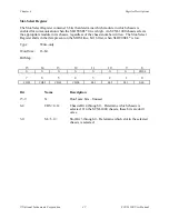
Bit
Name
Description (continued)
5
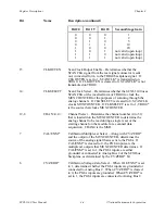
RTEMP
Read Temperature – Determines whether the PGIA output
or the MTEMP signal is driven onto the MCH0
±
pins of the
rear signal connector. If RTEMP is cleared to 0, the PGIA
output is used as the module output. If RTEMP is set to 1,
the MTEMP signal is the module output. The module
output is driven only when FOUTEN* is cleared to 0 or
SCANCON is active (low) while SCANCONEN* is
cleared.
4
RSVD
Reserved – Should always be written to 0.
3
SCANCLKEN*
Scan Clock Enable – Determines whether MUXCOUNTER
will increment on each clock signal (the clock source is
determined by CLKSELECT) or keep its loaded value. If
SCANCLKEN* is cleared to 0, MUXCOUNTER will be
clocked during scans. If SCANCLKEN* is set to 1,
MUXCOUNTER will not be clocked.
2
SCANCONEN
Scan Control Enable – When set to 1, enables the
SCANCON signal.
1
AB0EN
Analog Bus 0 Enable – Determines whether Analog Bus 0
on the SCXIbus drives MCH0 on the rear signal connector.
If AB0EN is cleared to 0, Analog Bus 0 does not drive
MCH0. If AB0EN is set to 1, Analog Bus 0+ drives
MCH0+ through a buffer and Analog Bus 0- is connected
to MCH0-.
0
FOUTEN*
Forced Output Enable – Determines whether the module
drives the MCH0
±
pins on the rear signal connector with
either the PGIA output or the MTEMP signal, depending
on the state of RTEMP. If FOUTEN* is cleared to 0, the
MCH0
±
pins are driven through a buffer by the PGIA
output or the MTEMP line. If FOUTEN* is set to 1, the
MCH0
±
pins are not driven by the PGIA or MTEMP,
unless SCANCON is active (low) and the SCANCONEN
bit is cleared. If the PGIA or MTEMP is driving the output
buffer, FOUTEN* drives Analog Bus 0 if AB0EN is set. If
nothing is driving the output buffer, the SCXI-1100 output
saturates.


