Memory Maps
MVME197LE/D2
3-5
3
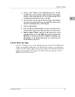
3. Writes to the LCSR in the VMEchip2 must be 32 bits.
LCSR writes of 8 or 16 bits terminate with a TEA signal.
Writes to the GCSR may be 8, 16, or 32 bits. Reads to the
LCSR and GCSR may be 8, 16, or 32 bits.
4. This area does not return an acknowledge signal. If the
processor bus timeout timer is enabled, the access times
out and is terminated by a TEA signal.
5. Size is approximate.
6. Port commands to the 82596CA must be written as two
16-bit writes: upper word first and lower word second.
7. DROM (BOOT ROM) appears at $0 following a local
peripheral bus reset. The DROM appears at 0 until the
DR0 bit is cleared in the PCCchip2. In addition, the
ROM0 bit in the BusSwitch must be cleared before
the DRAM is accessed.
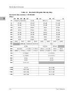
Detailed I/O Memory Maps
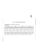
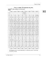
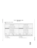
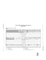
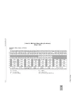
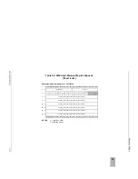
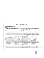
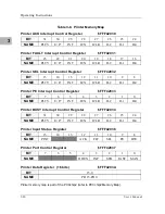
Tables 3-3 through 3-14 give the detailed memory maps for the BusSwitch
register, the ECDM CSR register, the DCAM (I
2
C) register, the VMEchip2
register, the PCCchip2 register, the printer register, the CD2401 Serial Port
register, the Ethernet LAN register, the SCSI Controller register, and the
BBRAM/TOD Clock register.
Содержание MVME197LE
Страница 1: ...MVME197LE Single Board Computer User s Manual MVME197LE D2 ...
Страница 12: ...xii ...
Страница 14: ...xiv ...
Страница 22: ...Hardware Preparation and Installation 2 2 User s Manual 2 ...
Страница 30: ...Hardware Preparation and Installation 2 10 User s Manual 2 ...
Страница 37: ...Memory Maps MVME197LE D2 3 7 3 ...
Страница 40: ...Operating Instructions 3 10 User s Manual 3 ...
Страница 42: ...Operating Instructions 3 12 User s Manual 3 ...
Страница 44: ...Operating Instructions 3 14 User s Manual 3 ...
Страница 46: ...Operating Instructions 3 16 User s Manual 3 ...
Страница 48: ...Operating Instructions 3 18 User s Manual 3 ...
Страница 60: ...Functional Description 4 2 User s Manual 4 ...
Страница 68: ...Functional Description 4 10 User s Manual 4 ...
Страница 78: ...Index IN 4 User s Manual I N D E X ...

