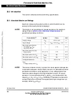
Electrical Specifications
3.0-V DC Electrical Characteristics
MC68HC908GP32
•
MC68HC08GP32
—
Rev. 6
Technical Data
MOTOROLA
Electrical Specifications
371
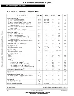
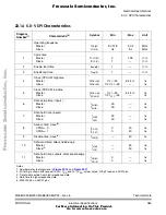
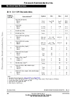
Low-voltage inhibit, trip falling voltage
V
TRIPF
2.45
2.60
2.70
V
Low-voltage inhibit, trip rising voltage
V
TRIPR
2.55
2.66
2.80
V
Low-voltage inhibit reset/recover hysteresis
(V
TRIPF
+ V
HYS
= V
TRIPR
)
V
HYS
—
60
—
mV
POR rearm voltage
(8)
V
POR
0
—
100
mV
POR reset voltage
(9)
V
PORRST
0
700
800
mV
POR rise time ramp rate
(10)
R
POR
0.02
—
—
V/ms
Notes:
1. V
DD
= 3.0 Vdc
±
10%, V
SS
= 0 Vdc, T
A
= T
L
to T
H
, unless otherwise noted
2. Typical values reflect average measurements at midpoint of voltage range, 25
°
C only.
3. Run (operating) I
DD
measured using external square wave clock source (f
OSC
= 16.4 MHz). All inputs 0.2V from rail. No
dc loads. Less than 100 pF on all outputs. C
L
= 20 pF on OSC2. All ports configured as inputs. OSC2 capacitance linearly
affects run I
DD
. Measured with all modules enabled.
4. Wait I
DD
measured using external square wave clock source (f
OSC
= 16.4 MHz). All inputs 0.2 V from rail. No dc loads.
Less than 100 pF on all outputs. C
L
= 20 pF on OSC2. All ports configured as inputs. OSC2 capacitance linearly affects
wait I
DD
. Measured with PLL and LVI enabled.
5. Stop I
DD
is measured with OSC1 = V
SS
.
6. Stop I
DD
with TBM enabled is measured using an external square wave clock source (f
OSC
= 16.4 MHz). All inputs 0.2V
from rail. No dc loads. Less than 100 pF on all outputs. All inputs configured as inputs.
7. Pullups and pulldowns are disabled.
8. Maximum is highest voltage that POR is guaranteed.
9. Maximum is highest voltage that POR is possible.
10. If minimum V
DD
is not reached before the internal POR reset is released, RST must be driven low externally until minimum
V
DD
is reached.
Characteristic
(1)
Symbol
Min
Typ
(2)
Max
Unit
F
re
e
sc
a
le
S
e
m
ic
o
n
d
u
c
to
r,
I
Freescale Semiconductor, Inc.
For More Information On This Product,
Go to: www.freescale.com
n
c
.
..


