Timer Interface Module (TIM)
Technical Data
MC68HC908GP32
•
MC68HC08GP32
—
Rev. 6
364
Timer Interface Module (TIM)
MOTOROLA
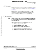
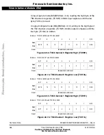
In input capture mode (MSxB:MSxA = 0:0), reading the high byte of the
TIM channel x registers (TCHxH) inhibits input captures until the low
byte (TCHxL) is read.
In output compare mode (MSxB:MSxA
≠
0:0), writing to the high byte of
the TIM channel x registers (TCHxH) inhibits output compares until the
low byte (TCHxL) is written.
Address: T1CH0H, $0026 and T2CH0H, $0031
Bit 7
6
5
4
3
2
1
Bit 0
Read:
Bit 15
14
13
12
11
10
9
Bit 8
Write:
Reset:
Indeterminate after reset
Figure 22-12. TIM Channel 0 Register High (TCH0H)
Address: T1CH0L, $0027 and T2CH0L $0032
Bit 7
6
5
4
3
2
1
Bit 0
Read:
Bit 7
6
5
4
3
2
1
Bit 0
Write:
Reset:
Indeterminate after reset
Figure 22-13. TIM Channel 0 Register Low (TCH0L)
Address: T1CH1H, $0029 and T2CH1H, $0034
Bit 7
6
5
4
3
2
1
Bit 0
Read:
Bit 15
14
13
12
11
10
9
Bit 8
Write:
Reset:
Indeterminate after reset
Figure 22-14. TIM Channel 1 Register High (TCH1H)
Address: T1CH1L, $002A and T2CH1L, $0035
Bit 7
6
5
4
3
2
1
Bit 0
Read:
Bit 7
6
5
4
3
2
1
Bit 0
Write:
Reset:
Indeterminate after reset
Figure 22-15. TIM Channel 1 Register Low (TCH1L)
F
re
e
sc
a
le
S
e
m
ic
o
n
d
u
c
to
r,
I
Freescale Semiconductor, Inc.
For More Information On This Product,
Go to: www.freescale.com
n
c
.
..


