第 16 页 共 60 页
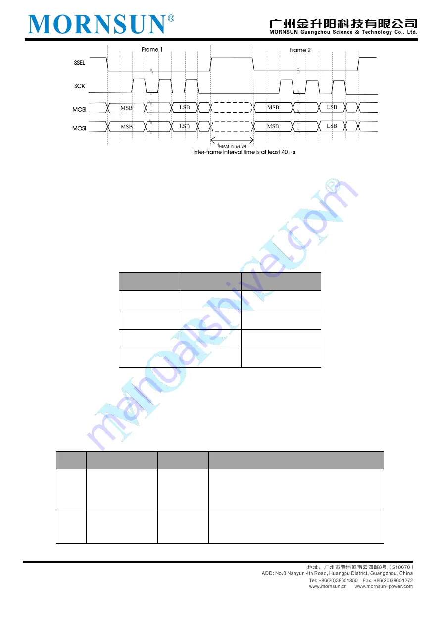
Figure 3.6 Schematic diagram of SPI frame interval
2. Master control
TD5(3)USPCAN has two SPI Master control pins CTL0 and CTL1, which are controlled by the master. By
controlling the CTL0 and CTL1 pins, the master make TD5(3)USPCAN enter different functional states, and
achieve different operation purposes for TD5(3)USPCAN. The corresponding functions of different levels of
mastercontrol pins are shown in Table 3.2.
Table 3.2 Master Control Function in SPI Mode
CTRL0
CTRL1
Function
0
0
Inactive
0
1
master read status
1
0
master read data
1
1
master write data
The master can read the current state of the slave to obtain the number of bytes that the product can
read and write. Select the master function as the master read state, and then read out 4 bytes through SPI,
which is the status code. The status code consists of 32 bits, and the specific definition is shown in Table 3.3.
Table 3.3 Composition of status codes in SPI mode
Bit
Meaning
Symbol
Describe
0
Readable
identification
bit
read
When the CAN receiving buffer is not
empty, this bit is 1, otherwise it is 0.
12:1
Number of
readable bytes
read_bytes
Number of bytes of CAN data that the
master can read from TD5(3)USPCAN.


