background image

52

Chapter 7. Digital I/O

H[IGH]

Count while input is

HIGH

, enables counter

L[OW]

Count while input is

LOW

, enables counter

R[ISING]

Count rising edges, enables counter

F[ALLING]

Count falling edges, enables counter

B[OTH]

Count both rising and falling edges, enables counter

The following

NSB

-mode example sets up a rising edge counter on

HSB3

and counts for approximately 100 ms.

1

EXTIO,MODE,2,HSB,READ
EXTIO,COUNTER,2,HS3,RISING
EXTIO,COUNTER,2,HS3,RESET
SLEEP,100

# wait approximately 100ms

EXTIO,COUNTER,2,HS3,READ

# returns counts recorded

7.8

Examples

The following examples demonstrate how to configure and use the

external I/O pins.

Note that pins must be set to

MANUAL

using the

EXTIO,CTRL

command to be used for

READ

and

WRITE

.

These commands may be useful in executing scripts or diagnosing

experiments.

For any application where timing is important, table

mode should be used.

EXTIO,CTRL,1,HSB,MAN

Set HSB1 to

MANUAL

mode, for use with

READ

and

WRITE

EXTIO,WRITE,1,DOUT,1

Sets the

CH1-DOut

pin (

DB15

) to

HIGH

EXTIO,READ,2,OFF

Reads the current state of the

CH2-OFF

pin (

DB15

)

EXTIO,MODE,1,HSB,WRITE

Set the entire first high-speed bank into write mode

1

Advanced table mode should be used for more accurate measurement (

§

9.4).

Содержание ARF021

Страница 1: ...Agile RF Synthesizer AOM driver ARF021 ARF421 XRF021 XRF421 Version 1 5 0 Rev 6 ...

Страница 2: ...e or use of any of its products The foregoing limitation of liability shall be equally applicable to any service provided by MOGLabs Copyright Copyright c MOG Laboratories Pty Ltd MOGLabs 2015 2018 No part of this publication may be reproduced stored in a retrieval system or transmitted in any form or by any means electronic mechanical photocopying or otherwise without the prior written permission...

Страница 3: ...y frequency amplitude and phase with high resolution Analogue modulation of each chan nel in frequency amplitude and or phase with 10 MHz bandwidth Ergonomic front panel controls and ethernet USB interface Table mode operation to define complex time dependent waveform output All in one box which connects directly to AC mains power and to your AOMs As you delve into this manual you will uncover mor...

Страница 4: ...ii ...

Страница 5: ...ety precautions that are standard for any electronic equipment CAUTION To ensure correct cooling airflow the unit should not be ope rated with cover removed WARNING High voltages are exposed internally particularly around the mains power inlet and internal power supply unit The unit should not be operated with cover removed NOTE The MOGLabs ARF XRF is designed for use in scientific re search labor...

Страница 6: ...h power RF output if not con nected or if a short circuit is detected Reflected power The RF reflected power and VSWR voltage standing wave ratio are monitored and RF output is disabled if either exceeds their safe limit settings Mains filter Protection against mains transients Temperature Several temperature sensors control the fan and will trigger a shutdown if the temperature exceeds a safe lim...

Страница 7: ...r panel controls and connections 8 2 3 Internal DIP switches 9 3 Communications 11 3 1 Protocol 11 3 2 TCP IP 13 3 3 USB 14 4 MOGRF host software 17 4 1 Device discovery 17 4 2 Device commander 18 4 3 MOGRF main window 19 4 4 Table viewer 24 4 5 External I O settings 25 5 External modulation 27 5 1 Operational principle 27 5 2 Modulation gain 28 5 3 Dual modulation fast and slow modes 29 v ...

Страница 8: ...ng timing 49 7 7 Counters 51 7 8 Examples 52 8 Simple table mode 55 8 1 Operational principle 55 8 2 Defining table entries 56 8 3 Digital I O 59 8 4 Loops and triggers 64 8 5 Upload and download 67 8 6 Re arm and restart 68 8 7 Linear ramps 69 8 8 Synchronous table execution 71 9 Advanced table mode XRF 73 9 1 Operational principle 73 9 2 Defining table entries 74 9 3 Initial and final states 78 ...

Страница 9: ...n XRF 98 C Command language 99 C 1 Arguments 99 C 2 General functions 100 C 3 Basic control 100 C 4 Primary RF control 101 C 5 Modulation 103 C 6 Digital ramp generator 104 C 7 Monitor outputs 106 C 8 Clock reference 107 C 9 Table mode 108 C 10 PID feedback 111 C 11 External IO functions 113 C 12 Configuration settings 115 C 13 Direct DDS control 116 D Code examples 119 D 1 python 119 D 2 matlab 1...

Страница 10: ...viii Contents ...

Страница 11: ...rol knobs or via a scripting language over ethernet or USB The RF parameters can be defined in a lookup table loaded via ethernet or USB to enable complex sequences with very fast transitions The block diagram below shows the key components The RF sig nal output from each DDS is low pass filtered pre amplified and FPGA Front Panel Display Control Local Oscillator Micro controller DDS RF AD9910 DDS...

Страница 12: ...ing complex waveform sequen ces where each step in the sequence can include frequency power phase time delay and more complex definitions of ramps and other time dependent functions Complex capabilities can be accessed via either TCPIP or USB communications See Chapter 3 for information on communications options and setup Once communications are established the ARF XRF can be controlled with simpl...

Страница 13: ...requires careful reference to the AD9910 datasheet and manual calculation of the hardware registers TSB Simple table mode In table mode the RF parameters are automatically sequenced by the FPGA according to a table of values pre loaded by the micro controller and stepped through automatically The table entries are defined by simple text commands from the host computer which de fine the RF frequenc...

Страница 14: ...witch before the amplifiers This hardware switch short circuits the RF output of the DDS and can be controlled via a combination of software and hardware inputs see 7 6 In this way the RF can be controlled using the front panel the ON OFF commands as well as via table entries with appropriate flags There is additional control of the DC supplies to the high power RF amplifiers to further improve th...

Страница 15: ...r activates the selected command The main menu Figure 2 1 shows the current mode and status of each channel In basic NSB mode the current frequency and power of each channel is displayed as well as whether modulation is cur rently enabled Pressing the OK button with a channel selected will open the sub menu to adjust settings for that channel Figure 2 2 The color of each menu item represents its p...

Страница 16: ... the table shown Figure 2 2 The basic parameters of each channel can be edited directly Turning the encoder wheel modifies the selected digit of the current value left as indicated by the arrow Pressing the encoder wheel changes to digit select mode right allowing the selected digit to be changed by turning the encoder Figure 2 3 The options menu allows configuration of various settings such as th...

Страница 17: ... interface including whether to enable DHCP and the fall back static IP address of the device When in use the network status is displayed on the display footer and once connected displays the current IP address Note that the Restart ethernet command must be used before changes in the ethernet menu will take effect Each channel of the device can be turned on or off using the push buttons on the lef...

Страница 18: ...tely buffered RF outputs for monitoring at 20 dBc to each main output when high impedance terminated AMP FREQ Each RF channel has two associated analogue inputs FREQ and AMP nominally for frequency and amplitude modulation The FREQ input can optionally be reconfigured to perform phase modulation These modulation inputs can be used for laser noise eater or frequency stabilisation applications see c...

Страница 19: ...ducting objects do not enter the unit CAUTION The cover should be left on to ensure proper airflow and cooling OFF ON 1 Normal operation Legacy firmware update mode 2 Disable FPGA Normal operation 3 Use factory settings Normal operation 4 Normal operation Factory reset DIP 1 Default OFF If switched ON the unit will start in legacy firmware upload mode Connect to the device using a web browser and ...

Страница 20: ...PROM and loaded on startup If invalid settings are saved to EE PROM disable DIP 3 to load factory defaults to facilitate debugging and diagnostics DIP 4 Default OFF Switch ON and reboot to restore the unit to factory settings Firmware for both microcontroller and FPGA as well as the EEPROM settings will be restored ...

Страница 21: ...a carriage return r ASCII 0x0D and new line n ASCII 0x0A Most terminal applications and drivers provide the ability to automatically append these characters when configured appropriately Statements are either commands or queries A command is a statement that causes some action to occur and the unit will re spond with either OK or ERR depending on whether the command succeeded or not For example FR...

Страница 22: ...e should wait for this response and check whether it indicates an error before continuing The python and LabVIEW bindings provided by MOGLabs take care of buffering and error checking automatically The mogcmd application which is available from the MOGLabs website as a standalone application or as part of the mogrf package provides a convenient interface for sending commands and receiving response...

Страница 23: ...es as follows Once configured these settings are stored in the non volatile memory of the unit and will be recalled in future However automatic address acquisition via DHCP is a simpler solution where available 1 From the main menu open Options Ethernet Settings 2 Select Static IP and use the encoder wheel to set the IP address of the device as required Note that pressing the encoder wheel changes...

Страница 24: ... COM port on the machine To determine the port number of the device go to Device Manager Start then type Device Manager into the Search box You should see a list of devices including Ports Figure 3 2 Figure 3 2 Screenshot of Device Manager showing that the ARF can be communicated with using COM4 The port number might change when plugging into a different USB port or after applying a firmware updat...

Страница 25: ...en the driver was not successfully installed If this occurs disconnect the device from the host computer reinstall the VCP driver then reconnect the USB cable The mogrf host software 4 automatically enumerates the availa ble COM ports when started making device identification simpler ...

Страница 26: ...16 Chapter 3 Communications ...

Страница 27: ...cation a device discoverer Figure 4 1 is initiated This program scans the COM ports of the host computer looking for an ARF XRF device and then scans the local network subnet Starting the application is then as simple as selecting the device and clicking Connect If your device is not listed recheck your connection and network settings If the network and or firewall blocks device discovery enter th...

Страница 28: ...y executed commands Figure 4 2 The Device commander window which permits the execution of individual instructions or of text files containing scripts Scripts are ASCII text files where each line corresponds to a com mand to be executed see Appendix D Clicking Run script triggers stepwise execution of such a script where the success of each sta tement is checked before executing the subsequent line...

Страница 29: ...s 1 Current operational mode of the channel Click to change mode by selecting from a list Note that advanced table mode will only appear on XRF units 2 Current frequency amplitude and phase in NSB mode Chan ging the value immediately updates the output 3 Controls are provided for specific table mode functionality Ta bles can be exchanged with internal FLASH memory or uploa ded downloaded from the ...

Страница 30: ...t 8 The status bar contains diagnostic information about the unit and connection 4 3 1 File menu Device command Starts the Device commander 4 2 for interactive execution of in structions to control the device Upload firmware Starts the firmware update application to upload and install updates on the device The procedure for applying firmware updates is des cribed in detail in Appendix B It is stro...

Страница 31: ...plication to be restarted and may also require the device to be rebooted The port should be unchanged at 7802 to ensure that the mogrf suite of programs can continue to communicate with the device Modulation The ARF XRF supports a wide variety of modulation options detailed in chapter 5 Individual modulation types can be enabled disabled and their gains adjusted Figure 4 5 Synchronisation Configur...

Страница 32: ...th high bandwidth on AM PID is disabled but constants have been set Download settings Downloads configuration and calibration data from the device and stores it in a file for backup purposes It is strongly recommended to download settings before applying firmware updates Upload settings Restore previously downloaded settings to the unit ...

Страница 33: ...th the device please run the diag nostics and click save results Please send the resulting text file and a description of the problem to MOGLabs for analysis Figure 4 6 Diagnostic information about the connected ARF unit which should be sent to MOGLabs for analysis if there is a problem with the device About Displays version information about the mogrf toolkit and connected ARF XRF device for supp...

Страница 34: ...Figure 4 7 Table viewer showing how the frequency power and phase of a table stored in FLASH memory change across the sequence left The example shown is a chirped Gaussian pulse with a number of rapid on off pulses at the beginning Mouse controls allow zooming in on areas of interest such as the rapid pulses at the start of the sequence right At present the table viewer is only available for simpl...

Страница 35: ...ed in table mode Figure 4 8 External I O configuration window showing the current state of inputs yellow outputs green table mode outputs blue and disabled outputs black Left clicking on an output changes its state and right clicking brings up a menu of options Features of the EXTIO configuration window are 1 Current state of the input pins of the DB15 connector note that SEQ is disabled on Rev2 u...

Страница 36: ... two high speed banks The banks are di sabled black on boot and must be set to either read yellow or write green mode on a per bank level However individual output pins can be set as Auto blue for use in table mode by right clicking each indicator 6 Mode to apply to the associated high speed bank Note that Read mode is not available on Rev2 units ...

Страница 37: ...nal which is then multiplied by the modulation gain and added to the in ternal control value associated with the particular modulation mode frequency tuning word for frequency amplitude scale factor for power or phase offset word for phase Limits are applied to the value to ensure that the power is always limited to the value set with the LIMIT command The DAC operates at 62 5 MS s with 12 bit res...

Страница 38: ...Max gain dec 1 073 709 056 16 383 65 535 Step size 0 23 Hz 0 006 Max 0 0055 Max modulation 250 MHz 100 Max 360 Table 5 1 Gain ranges for different modulation modes Based on these values and ignoring discretisation and saturation an applied voltage will have the following effective modulation Frequency df 0 23 Hz V Gf Vin Phase dφ 0 0055 V GφVin Amplitude dA 14 V V GaVin for 421 models 2 6 V V GaVi...

Страница 39: ...21 at an average RF power of 30 dBm use the POW command to determine that the amplitude is 0x2000 8192 and set the gain to 8192 0 5 4096 5 3 Dual modulation fast and slow modes The ARF XRF is capable of dual modulation where the RF is either simultaneously FM and AM or PM and AM modulated However due to DDS interface limitations only one parameter can be modulated at full speed using the parallel ...

Страница 40: ...tly supported as phase mo dulation shares the FREQ modulation input 5 4 Examples 5 4 1 Simple linear ramps Listing 5 1 shows how to use the MOD OUT connector on the rear panel to linearly ramping the RF amplitude and frequency simulta neously Figure 5 1 Ensure that MOD OUT is connected to both the FREQ1 and AMPL1 modulation inputs in parallel Subsequently increasing the AM gain results in clamping...

Страница 41: ... of simultaneous AM FM modulated RF red when the modulation inputs are driven by the SLHRAMP monitor output blue Figure 5 2 Demonstration of high gain amplitude modulation showing clipping at zero and the power limit set by the LIMIT command ...

Страница 42: ... When FMSPEED is set to FAST the amplitude is modulated using the slow serial interface and the enve lope displays large stepwise discretisation However when FMSPEED is SLOW amplitude modulation uses the parallel interface and the resulting envelope is smoother Figure 5 3 Comparison of slow top and fast bottom amplitude modu lation for a 100 kHz sine wave modulation input ...

Страница 43: ...chieved with a 2 Vpp modulation input with gain 0x7fff or a 1 Vpp modulation input with gain 0xffff Figure 5 4 Figure 5 4 A 1 Vpp 10 kHz triangle wave blue is used for phase mo dulation of CH1 and demodulated with an unmodulated CH2 at the same frequency magenta Note that it may be necessary to adjust the phase of one of the chan nels using the PHAS command to compensate for differential phase del...

Страница 44: ...34 Chapter 5 External modulation ...

Страница 45: ...eference such as a high finesse cavity 6 1 Signal conditioning Upon engaging the PID controller the associated modulation input SMA connector on the back panel is treated as an error signal instead of a control voltage and the action of the controller is to drive this signal towards zero However in applications such as intensity stabilisation it is desirable that the laser beam power as measured o...

Страница 46: ...roportional integral differential function u t Gkpe t Gki Z t 0 e τ dτ Gkd de dt where e t is the input error signal u t is the feedback response and G is the overall modulation gain The gain constants kp ki kd are floating point values in the range 0 1 which correspond to proportional integral and differential terms respectively Typical values are kp 0 03 0 8 ki 0 01 0 15 and kd 0 Earlier version...

Страница 47: ...Q 0x3FFFF set PID gains and enable PID GAIN 1 P 0 1 PID GAIN 1 I 0 01 PID GAIN 1 D 0 PID ENABLE 1 AMPL set FM to SLOW mode allowing PID to be FAST FMSPEED 1 SLOW Listing 6 1 Simultaneous FM and PID intensity stabilisation example Limitations of the DDS interface mean that only one of PID and external modulation can be performed at full bandwidth 5 3 Most applications will benefit from using PID in...

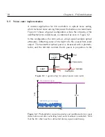
Страница 48: ...enuator diffracting some of the light into the unused first order output The transmitted optical power is measured with a photode tector and the ARF XRF controls the RF power in proportion to the Photodetector AOM Laser Stabilised Offset ARF XRF Beamsplitter Error Figure 6 1 Typical setup for optical power noise eater Time Time Volts Offset Photodetector signal ARF XRF input error signal 1 2 3 4 5...

Страница 49: ...e that the gain constants must be tuned for each particular implementation Optimising the gain constants in real time with the Modulation settings window in mogrf 4 3 2 while monitoring the measured noise on a spectrum analyser is re commended for optimal performance Setup channel 1 for PID noise eater feedback set sample rate PID RATE 1 15 625 set P I D A gains PID GAIN 1 P 0 5 PID GAIN 1 I 0 05 ...

Страница 50: ...40 Chapter 6 PID stabilisation ...

Страница 51: ...Pin 13 Ch2 Analogue outputs for diagnostics and monitoring controlled by the MOUT command Note that the channel number here refers to the DAC channel which is not necessarily the same as the RF channel CHx DOUT Pin 4 Ch1 Pin 9 Ch2 TTL outputs that can be controlled manually or from table mode for example to activate a mechanical optical shutter or trigger another device This output has a rise time...

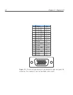
Страница 52: ...1 DOUT TTL out 5 CH2 SEQ TTL in 6 CH2 ON TTL in 7 CH2 OFF TTL in 8 GND 0 V 9 CH2 DOUT TTL out 10 GND 0 V 11 CH1 AOUT 2 5 V 12 GND 0 V 13 CH2 AOUT 2 5 V 14 GND 0 V 15 GND 0 V Figure 7 1 Pinout of high density 15 pin female D style rear panel IO connector Pins marked are not available in Rev2 units ...

Страница 53: ...ected the RF output will not turn on 7 2 High speed digital The FPGA also provides 16 high speed digital I O lines for use with table mode Internal connector P1 accepts a 30 way 0 50 mm pitch ribbon cable that can be inserted through a slot in the left hand side of the case The connector is an Omron XF2M 3015 1A with example matching FFC ribbons Molex 0982660326 150 mm length or 0152660329 200 mm ...

Страница 54: ...e can be inserted upside down reversing the pin ordering Version Driver Bank size Example configuration Rev2 74LVT2244 Outputs only 16x outputs Rev3 4 74LVTH2245 Banks of 8 8x inputs 8x outputs Rev5 74LVTH162245 Sub banks of 4 4x inputs 12x outputs Table 7 1 High speed I O configuration options Rev5 hardware can either configure the banks of 8 pins as above or control sub banks of 4 lines For exam...

Страница 55: ... connector left and high speed digital connector right The flat flex cable FFC carrying the high speed digital I O signals can be inserted in either orientation with contacts facing up or down Each pin of the high speed bus has two labels corresponding to the purpose of the pin given the cable orientation If the orientation is the same within the ARF XRF and the XSMA board the second set of labels...

Страница 56: ...a whole bank HSBANK in case multiple outputs need to be changed simultaneously HSB is short hand for HSBANK Function OFF ON SEQ DOUT HSB HSn Enable X X Disable X X Reset X X X Mode X X Control X X X Write X X X Read X X X X X Counter X X The different EXTIO commands are summarised below EXTIO ENABLE EXTIO ENABLE ch pin Enable the functionality of the specified pin on the given channel ch If pin is...

Страница 57: ...bank is not in write mode the sub bank is changed to write mode first EXTIO WRITE EXTIO WRITE ch pin value Write the specified value to the output pin If pin is HSB then value is an 8 bit number whose bits correspond to the values to set on the pins of that bank Otherwise value can be one of ON OFF 1 or 0 If the pin is not set to MANUAL control it is changed to manual control first EXTIO READ EXTI...

Страница 58: ...our CHx ON When the output is off pulling this pin LOW will switch both the RF signal and amplifiers ON NSB mode only Does not need enabling in software has no effect when disconnected CHx OFF When enabled see below the RF signal will be disabled unless this pin is pulled LOW If disconnected or TTL HIGH no output is generated Does not affect the RF amplifiers Because the CHx OFF input disables the...

Страница 59: ...n the DB15 connector or using amplitude modulation AM Note that when ge nerating pulses using AM the input tolerance is 1 V whereas the TTL inputs are 5 V tolerant Typical delays are shown in Table 7 2 Pulses can also be easily generated in a preprogrammed sequence using table mode chapter 8 Table mode pulses on ARF devices are limited to a minimum duration of 1 µs whereas the XRF is capable of th...

Страница 60: ...e delays for switching hardware components and for different methods of pulse generation The time given for ampli fier transitions includes time for the output to stabilise which may vary between hardware revisions Figure 7 4 Modulation of RF output using the CHx OFF input Green is TTL signal at the source blue is the TTL signal at the RF switch internal to ARF magenta is the RF signal ...

Страница 61: ...er the associated pin must be in READ mode and the counter function activated The maximum edge detection rate on the high speed bus is 50 MHz and level detection HIGH and LOW modes accumulates 125 counts per microsecond The syntax to control counters is EXTIO COUNTER ch pin command where command is one of the following READ V ALUE Return the counter value as a 32 bit number RESET C LEAR Reset the ...

Страница 62: ...AD returns counts recorded 7 8 Examples The following examples demonstrate how to configure and use the external I O pins Note that pins must be set to MANUAL using the EXTIO CTRL command to be used for READ and WRITE These commands may be useful in executing scripts or diagnosing experiments For any application where timing is important table mode should be used EXTIO CTRL 1 HSB MAN Set HSB1 to M...

Страница 63: ...ns in HSB1 Sets pins 0 2 HIGH and pins 3 7 LOW EXTIO MODE 2 HSB READ Sets the entire second high speed bank into read mode only available in Rev3 models EXTIO READ 2 HSB Simultaneously read all 8 inputs of the second HSB and return the result as an 8 bit number EXTIO READ 2 HS3 Read only port 3 of HSB2 returns ON or OFF ...

Страница 64: ...54 Chapter 7 Digital I O ...

Страница 65: ... rf output at each step as well as any desired I O These are preloaded by the FPGA into a DDS profile so that when the sequence is executed the parameters are updated instantaneously The speed of the serial interface limits the rate at which new in structions can be loaded into the DDS so the duration of each table entry is discretised at 1 µs 1 Once the sequence has been defined using the TABLE E...

Страница 66: ...grade and tables should be archived in human readable form When a table is armed the RF is switched on including the ampli fiers for 421 models and upon completion of the table the final RF state remains ongoing If it is required that the output be disabled when the table is complete the final entry should set the power to 0x0 zero amplitude not 0 dBm 8 2 Defining table entries Table entries can b...

Страница 67: ...operation can be performed in a given table entry IOSETx Write multiple HSB digital outputs simultaneously 8 3 2 in con junction with an IOMASK flag IOMASKy Specifies which outputs should be controlled by IOSET 8 3 2 The following commands are also provided to simplify editing tables in memory They take the same parameters as the TABLE ENTRY command but automatically update the table entry count a...

Страница 68: ...ompletes so it is good practice to include a final instruction that sets the output power to minimum Example of table output MODE 1 TSB Begin table TABLE ENTRY 1 1 100MHz 10dBm 0 100 TABLE ENTRY 1 2 100MHz 0dBm 0 100 TABLE ENTRY 1 3 80MHz 5dBm 0 100 TABLE ENTRY 1 4 80MHz 15 0dBm 0 100 TABLE ENTRY 1 5 100MHz 2 0dBm 0 100 TABLE ENTRY 1 6 100MHz 0x0C00 0 100 TABLE ENTRY 1 7 100MHz 0x0200 0 100 TABLE ...

Страница 69: ...t DOUT associated with this channel on the DB15 connector 0 7 The specified pin of the high speed bank with the same number as this channel A for CH1 B for CH2 A0 A7 The specified pin of high speed bank A irrespective of channel B0 B7 The specified pin of high speed bank B irrespective of channel Both channels are capable of accessing the same I O pins using the second notation It is up to the use...

Страница 70: ...0 2 next entry sets pin 1 high TABLE ENTRY 1 2 100MHz 0x600 0 2 IO1H 2us later set pin 1 low TABLE ENTRY 1 3 100MHz 0x1000 0 2 IO1L TABLE ENTRY 1 4 100MHz 0x1400 0 2 create 500ns pulse TABLE ENTRY 1 5 100MHz 0x2000 0 2 IO1P TABLE ENTRY 1 6 100MHz 0x200 0 2 toggle pin 1 from low to high TABLE ENTRY 1 7 100MHz 0x600 0 2 IO1T TABLE ENTRY 1 8 100MHz 0x1000 0 2 toggle pin 1 again i e from high to low T...

Страница 71: ...oth high speed banks to be changed in each table entry or only a subset of the pins Table 8 1 demonstrates an example that simultaneously writes 5 pins of bank A and 4 pins of bank B Bank B Bank A Bit 16 15 14 13 12 11 10 9 8 7 6 5 4 3 2 1 IOSET 0 0 1 0 1 1 1 1 1 0 0 1 0 0 1 1 IOMASK 0 1 0 0 1 1 0 1 1 1 1 0 1 0 1 0 Outcome 0 1 1 1 1 0 0 0 1 Table 8 1 Example of simultaneous output using IOSET0x2F9...

Страница 72: ...L IOB1H which is equivalent to IOSET0x0208 IOMASK0x0218 but has improved clarity Note Multiple digital output mode cannot be used in combination with LOOP or TRIG 8 3 3 External trigger The TRIG flag indicates that the current instruction should be repe ated until a hardware trigger is received The source and trigger condition can also be specified using the syntax TRIGxy where x is the pin 8 3 1 ...

Страница 73: ... external trigger on the DB15 input in this instance it is not necessary to specify the TRIG flag on the first table entry If a trigger is not received the TABLE STOP command must be used to abort operation Examples of trigger flags TRIG Continue on a falling edge on the DB15 input TRIGDH Continue if the DB15 input is logic HIGH TRIGA3R Continue on a rising edge on high speed pin A3 The example be...

Страница 74: ...ronise with external devices TABLE LOOP TABLE LOOP ch source dest condition Set the table to loop between the source and dest instructions until the condition is satisfied If source and dest are the same or if dest is 0 then the table effectively holds the instruction source and dest can be negative numbers which are then taken as offsets If source is negative it is taken as an offset from the end...

Страница 75: ...e loop after rising edge occurs The TRIG flag of the TABLE ENTRY command is short hand notation for TABLE LOOP using the IODF condition and therefore the same re strictions apply Loops are subject to the following restrictions Nested loops are not supported The TABLE LOOP command can only be used after the source entry has been defined The first and last entries of the table cannot contain a LOOP ...

Страница 76: ...0MHz 5dBm 0 4us TABLE ENTRY 1 3 100Mhz 10dBm 0 2us TABLE LOOP 1 3 1 4 TABLE ENTRY 1 4 100MHz 30dBm 0 1us Listing 8 3 Demonstration of a simple loop Figure 8 4 Demonstration of a simple loop An alternate way of specifying the LOOP instruction in the above example is TABLE LOOP 2 3 4 as the TABLE ENTRIES was already set to 4 so source 2 corresponds to entry 3 and the destination is 3 instructions ea...

Страница 77: ...commended that all tables be stored in ASCII human readable format for long term storage An example of this format is shown below 100 MHz 5 dBm 0 deg 10us 150 MHz 0 dBm 90 deg 2us IODH 80 MHz 5 dBm 0 deg 1us TRIG 100 MHz 0 dBm 0 deg 5us Listing 8 4 Example of table mode CSV file for use with mogrf A distinction should be made between CSV tables and scripts In this context CSV tables contain only t...

Страница 78: ...ORESET option will prevent resetting the DDS phase accumulator between executions and reduces the delay Note that unless the NORESET option is enabled the output will be switched off during the phase accumulator reset 2µs If this delay is unacceptable an alternative is to specify a loop back to the beginning of the sequence using the TABLE LOOP command which will repeat the table with no delay As ...

Страница 79: ...es are generated whereas in advanced table mode only 3 entries are required For example the command TABLE RAMP 1 FREQ 80 100 100us 2000 in TSB mode will generate 2000 table entries corresponding to a fre quency ramp that sweeps the RF frequency from 80 MHz to 100 MHz in a total time of 200 ms each step being 10 kHz and taking 100 us The command can also be used to specify piecewise linear envelope...

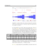
Страница 80: ...mps that can be watched on a spectrum analyser A graph of the corresponding frequency of the RF over time is shown in Figure 8 6 MODE 1 TSB TABLE CLEAR 1 set initial conditions TABLE APPEND 1 80MHz 0dBm 0 1us define first ramp TABLE RAMP 1 FREQ 70 80 1m 1000 append a pause TABLE APPEND 1 80 5dbm 0 1s append second and third ramps TABLE RAMP 1 FREQ 80 75 5m 200 TABLE RAMP 1 FREQ 75 85 2m 500 Listin...

Страница 81: ...he command TABLE SYNC 1 This configures CH1 as the master and CH2 as the slave such that the CH2 DDS derives its clock from the CH1 DDS for phase stability Once enabled CH2 cannot be started independently of CH1 and CH1 cannot be started unless CH2 has been armed For this reason it is recommended to activate the auto rearm feature on CH2 using the command TABLE REARM 2 1 The feature must be deacti...

Страница 82: ...ible to synchronise the DB15 triggers received by the two tables The two trigger inputs on the DB15 connector can be hardwired together but the FPGA can also be instructed to trig ger both channels from the same input This functionality can be controlled by the TABLE TRIGSYNC command This does not apply to the high speed bus as both tables can be instructed to use the same input as a trigger regar...

Страница 83: ...are therefore two kinds of instructions in advanced mode parallel and serial Parallel instructions allow a single parameter to be updated rapidly whereas serial instructions are preloaded into the serial interface and then activated in a subsequent command This load activate cycle allows changes to be made to the parallel parameter without having to wait for the serial load to complete Advanced mo...

Страница 84: ...ds which is identical to simple table mode syntax 2 TABLE XPARAM TABLE XPARAM ch param fmgain Sets which parameter is to be controlled on the parallel interface Must be called before the table is populated with entries The parameter is one of FREQ PHAS POW or AMPL The parameters POW and AMPL are synonyms in this mode Subsequent PIF table entries can then modify this parameter When entering FREQ mo...

Страница 85: ...TABLE APPEND 1 POW 5dbm 16ns TABLE APPEND 1 POW 10dbm 50ns TABLE APPEND 1 POW 0dbm 16ns TABLE APPEND 1 POW 40dbm 16ns Listing 9 1 Parallel instruction example in advanced table mode Figure 9 1 Output generated by Listing 9 1 Parallel mode instructions also provide functionality for piecewise linear interpolations as described in 9 6 This enables the creation of smooth ramps without requiring a lar...

Страница 86: ... and the update flag must be at least 960ns otherwise the DDS does not have time to load the instructions However any flags specified in the instruction such as digital output will occur immediately The example below demonstrates how to queue and then activate a serial instruction in advanced table mode define a SIF entry using simple mode syntax TABLE APPEND 1 100MHz 5dbm 0 1us trigger the update...

Страница 87: ...other parallel instruction at new frequency TABLE APPEND 1 POW 5dbm 100ns final instruction to power down TABLE APPEND 1 POW 0x0 0x1 Listing 9 3 Demonstration of parallel instructions during a SIF load Figure 9 2 Output generated by Listing 9 3 Note The value corresponding to the parallel parameter is ignored when loading a serial update and must be set separately For example in Listing 9 2 the ou...

Страница 88: ... start condition TABLE APPEND 1 80MHz 5dbm 45deg 976ns OFF activate the update TABLE APPEND 1 POW 5dbm 16ns UPD 1us has elapsed up to here other table mode entries add a final entry to reset rf state TABLE APPEND 80MHz 5dbm 45deg 1us activate the update and turn off the rf TABLE APPEND 1 POW 30dbm UPD OFF Listing 9 4 Setting initial and final states in parallel mode The RF state at the last instru...

Страница 89: ...s a counter 7 7 before arming the table and each command takes effect at the start of each table instruction CxS TART Reset counter x to zero and then begin counting CxP AUSE Disable counter x and stop accumulating counts CxR ESUME Re enable counter x and resume accumulating counts CA LL Stop and reset all counters The parameter x in each of these flags is the counter pin such as A3 for pin 3 of b...

Страница 90: ...hen read back the count SLEEP 10 TABLE STATUS 1 EXTIO COUNTER 1 HS1 READ Listing 9 5 Demonstration of configuring HSA1 as a counter and control ling it in advanced table mode 9 5 Loops and triggers Loops and triggers can be specified in advanced table mode using the TABLE LOOP command and syntax as for simple table mode 8 4 However some different restrictions apply to loops in advanced table mode ...

Страница 91: ...e REPn flag in a table entry using the syntax shown below TABLE ENTRY 3 TABLE ENTRY ch num param delta duration REPn flags Sets the associated table entry to EXTRAPOLATE adding delta to the parameter param on each execution The instruction is repeated n times as specified by REPn The delta argument should be specified in hexadecimal when extra polating power amplitude as in this example Hexadecima...

Страница 92: ...1 POW set power to OFF TABLE APPEND 1 POW 0x0 0x1 linear ramp up 100 steps TABLE APPEND 1 POW 0x10 0x1 REP100 linear ramp down 100 steps TABLE APPEND 1 POW 0x10 0x1 REP100 reset power to OFF TABLE APPEND 1 POW 0x0 0x1 loop the ramp 2 more times TABLE LOOP 1 1 1 2 last entry cannot be loop TABLE APPEND 1 POW 0x0 0x1 Listing 9 6 Creation of a triangle wave envelope in advanced table mode using only ...

Страница 93: ...frequency 32 bits This is an inherent restriction of the DDS so in order to specify frequency on the parallel interface gain is applied by the DDS when receiving the instruction which amounts to a bit shift of the incoming value Figure 9 4 LSB MSB 0 11 30 26 FM gain 11 16 bit parameter Figure 9 4 Visualisation of how FM gain allows the frequency word to be modified by the 16 bit parallel bus In th...

Страница 94: ...eved in advanced table mode is f0 dfmax where f0 is the center frequency set with the FREQ command and dfmax is the value in the above table correspon ding to the gain To assist with understanding these ranges the TABLE XPARAM ch FREQ command will output information about what combinations are possible for the current set of parameters Note that the frequency gain can presently only be set before ...

Страница 95: ...quent instruction containing the UPD flag to activate them HOLD Do not change the output also known as a nop or no operation Intended to perform I O operations or trigger a serial update using the UPD flag without changing the RF REGx Write a 32 bit value directly to register x of the DDS using the serial interface Provided for advanced functionality in consultation with the AD9910 datasheet Requi...

Страница 96: ...LE APPEND 1 POW 18 88dBm 0x1 TABLE APPEND 1 POW 14 99dBm 0x1 TABLE APPEND 1 POW 10 53dBm 0x1 TABLE APPEND 1 POW 5 74dBm 0x1 TABLE APPEND 1 POW 0 95dBm 0x1 TABLE APPEND 1 POW 3 41dBm 0x1 TABLE APPEND 1 POW 6 92dBm 0x1 TABLE APPEND 1 POW 9 21dBm 0x1 TABLE APPEND 1 POW 10 00dBm 0x1 TABLE APPEND 1 POW 9 21dBm 0x1 TABLE APPEND 1 POW 6 92dBm 0x1 TABLE APPEND 1 POW 3 41dBm 0x1 TABLE APPEND 1 POW 0 95dBm ...

Страница 97: ... using the instructions for the first The amplitude steps are specified in hexadecimal so that the EXTRAPOLATE feature can be used MODE 1 TPA TABLE CLEAR 1 serial load and trigger first frequency TABLE APPEND 1 40MHz 0dbm 0deg 1us TABLE APPEND 1 HOLD 0x1 UPD begin serial load of second frequency TABLE APPEND 1 120MHz 0dbm 0deg 0x1 define smooth pulse envelope using EXTRAPOLATE TABLE APPEND 1 POW 0...

Страница 98: ...APPEND 1 POW 0x153 0x1 REP3 TABLE APPEND 1 POW 0x0d1 0x1 REP3 TABLE APPEND 1 POW 0x06a 0x1 REP3 TABLE APPEND 1 POW 0x01f 0x1 REP3 trigger the frequency change TABLE APPEND 1 HOLD 0x1 UPD loop back to create second pulse TABLE LOOP 1 1 4 1 TABLE APPEND 1 POW 0x0 0x1 Listing 9 9 Back to back shaped pulses with different frequencies Figure 9 6 Two 1µs Gaussian pulses generated in advanced table mode ...

Страница 99: ... for triggering EXTIO CTRL 1 HSB AUTO change to FREQ mode and set the FM gain TABLE XPARAM 1 FREQ 15 step through a number of frequencies TABLE APPEND 1 FREQ 20 0x5 IOA1H TABLE APPEND 1 FREQ 40 0x5 IOA1L TABLE APPEND 1 FREQ 80 0x5 IOA1H TABLE APPEND 1 FREQ 160 0x5 IOA1L Figure 9 7 Example showing phase continuity with stepwise changes in frequency between 20 MHz and 400 MHz in advanced table mode ...

Страница 100: ...90 Chapter 9 Advanced table mode XRF ...

Страница 101: ...1 ppm 0 to 50 C Phase 0 to 2π 16 bit resolution Phase noise 120 dBc 1 kHz Signal to noise 80 dBc 30 dBm Intermodulation and spurious 80 dBc Channel crosstalk 90 dBc Power RF off 70 dBm Analogue input output Inputs 2 per channel 4 total Function FM AM φ or analogue sampling Sensitivity 1 V Bandwidth 10 MHz with 7th order anti alias Resolution 12 bit 65 MHz sampling rate DAC analogue out 3 channels ...

Страница 102: ...n in 0 5 V Table mode Min step size 1 µs basic table 16 ns advanced table Max table length 8191 instructions per channel FLASH memory Non volatile storage of up to 4 tables Trigger options Software or TTL via DB15 connector Channel sync Independent execution shared trigger or fully synchronised Mechanical power Display 128x64 pixel LCD with white backlight Fans 4 x temperature controlled fans 421 ...

Страница 103: ... on USB In these cases the legacy interface B 4 must be used WARNING Do not attempt to communicate with the ARF XRF while a firmware up grade is being applied and do not interrupt an upgrade or factory reset in progress B 1 Firmware components There are four distinct firmware images on each ARF XRF 1 UC primary microcontroller 2 IAP microcontroller boot loader 3 DISP the interactive front panel di...

Страница 104: ... reset Once the reset is complete upgrade can be reattempted to gain access to newer features or a different firmware can be applied Please contact MOGLabs if you encounter any difficulties during firmware upgrade B 3 Upgrade via mogrffw The recommended way to install updates is using the mogrffw application which is distributed as part of mogrf It can be star ted from within mogrf or as a separat...

Страница 105: ...hich upgrades are required Figure B 2 Each component of the firmware is compared against the package version and colour coded as follows Green Component matches package version and is up to date Yellow Package contains an update which should be applied Magenta Package contains an older version than currently installed Installing this component will downgrade the firmware which may be required if f...

Страница 106: ... to make room for the new image 2 The data is uploaded to the device 3 The device checks the data is received for consistency to en sure the upload was successful 4 The device is rebooted to load the new firmware The device will reboot after every individual component upgrade to ensure the upload was successful before moving on to the next com ponent mogrffw will automatically try to reconnect to ...

Страница 107: ...gurable but by default are UserID moglabs Password agilerf 6 Select Browse and then select the microcontroller firmware file The required file is a bin file inside the firmware zip file beginning with B3010 and including either R2 for Rev2 hardware or R3 for Rev3 It is very important that the correct file is uploaded do not select the file marked IAP 7 Click on Upload 8 The LCD display will indica...

Страница 108: ...s program Running the application and connecting to the unit provides the necessary information that needs to be sent to MOGLabs to acquire an activation code that unlocks this functionality in the unit Figure B 3 The application used to upgrade an ARF into an XRF Note that activation is unit specific and a separate activation code must be obtained for each device Also note that the firmware on th...

Страница 109: ...moglabs com In particular code written for firmware before v1 0 may need up dating to be compatible with newer releases please refer to the individual commands below C 1 Arguments Most commands require a channel number ch either 1 or 2 and accept a comma separated list of parameters Parameters shown in square brackets are optional and most commands are treated as queries when called without a valu...

Страница 110: ...causing unit to reboot Note that all communications links will be immediately closed CLOSE QUIT Close communications channel HELP List available commands INFO Report information about the unit VERSION Report versions of firmware currently running on device Please include this information in any correspondance with MOGLabs TEMP Report measured temperatures and fan speeds VMON Report diagnostic moni...

Страница 111: ...he specified channel des cribing whether the signal and amplifiers are switched on Returns an error if the device is not operational SLEEP SLEEP dt Pause microcontroller operation for dt milliseconds Intended for use in simple scripts to wait for a short amount of time e g for tables to finish execution C 4 Primary RF control FREQUENCY FREQ ch value NSB TPA modes only Set channel ch to specified f...

Страница 112: ...0 mW POW 1 24 dBm POW 1 23 9 LIMIT LIMIT ch value Defines absolute maximum RF power for given channel ch with the same syntax as the POW command This limit is applied within the FPGA to prevent damage to attached components and cannot be exceeded even by modulation If the limit is set below the current power level the current power is reduced to the limit The default limit is 27 dBm about 500 mW f...

Страница 113: ... PHRESET Simultaneously activates and then releases the phase accumulator reset of each DDS This ensures the phase of the two channels is well defined even if there is a fixed phase shift between them C 5 Modulation MSTAT MSTAT chan Reports the current modulation status for the specified channel For example issuing MSTAT 1 may return the response PID OFF FM SIF PM OFF AM PIF indicating that both A...

Страница 114: ...LMOD ch type value Return or set the zero offset calibration of the modulation input ADCs The ADCs may return a small nonzero value when zero volts is app lied to the input causing a small unintended shift in the modulation parameter The zero offset calibration corrects thus by subtracting the calibration from the measured value before performing modula tion The parameter type is either FREQ or AM...

Страница 115: ... which is necessary before executing the ramp again More advanced behaviour is possible using the DDS registers directly RAMPTRIG RAMPTRIG ch value Sets the trigger mode of the ramp Possible trigger settings are as follows only the first letter is significant EXT HW The DDS waits for a hardware trigger on the CHx OFF pin before executing the to ramp AUTO CONT Execute the ramp continuously once a r...

Страница 116: ...artfreq or endfreq is greater RAMPHOLD RAMPHOLD ch value Pauses or unpauses a currently executing parameter ramp Should only be called on a ramp in progress and not as a software timed trigger for ramp execution C 7 Monitor outputs A number of monitoring waveforms can be output for testing and diagnostic purposes including monitoring of the RF output powers and the PID loop MOUT MOUT ch type Sets ...

Страница 117: ... clock and stabilises with an internal phase locked loop PLL allowing synchronisation with other devices CLKSRC CLKSRC source ppln Query or set the current clock source source is either INT to use the internal 20 MHz oscillator or EXT to use the reference provided to the CLK IN connector on the back panel compatible with a number of standard reference frequencies such as a 10 MHz GPS clock When us...

Страница 118: ...out the status of the internal clocks When supplying an external clock check the diagnostic information to ensure that the clock input is registering correctly and is enabling a stable system clock C 9 Table mode Table mode gives access to the powerful sequencing functionality of the ARF XRF devices chapter 8 XRF devices also have access to advanced table mode chapter 9 which is controlled using t...

Страница 119: ... disabled with the OFF command REARM TABLE REARM ch on off Enables disables the automatic re arming loading of the table upon completion such that it can be started again without using the ARM command Table will then begin executing upon a software or hardware trigger RESTART TABLE RESTART ch on off Enables disables an automatic software controlled restart of the ta ble upon completion Automatical...

Страница 120: ...S counter DELETE TABLE DELETE ch num Deletes the specified table entry shifting all subsequent entries up and decrements the TABLE ENTRIES counter RAMP TABLE RAMP ch param start stop duration count Creates a linear ramp in param which is one of FREQ AMPL or PHAS from start to stop in count steps each lasting duration In simple table mode this generates count table entries whereas in advanced table...

Страница 121: ...RESET TABLE NORESET ch onoff Disables table mode phase reset for the specified channel Nor mally the DDS phase accumulator is reset when the table is started ensuring that the output waveform has the same starting phase for every execution However this requires switching off for a few mi croseconds while the DDS is reset which is undesirable for some applications Using NORESET will ensure the outp...

Страница 122: ...GE PID AVERAGE ch on off Enables disables averaging of the input control signal The digiti sers operate at much higher rates than the PID sampling rate With averaging on the extra measurements contribute to an average sig nal which is reset at the sampling rate If averaging is off the additional measurements are discarded DCBLOCK PID DCBLOCK ch on off Enables disables DC block which allows the err...

Страница 123: ... of the pin Example EXTIO ENABLE 1 OFF The pin parameter can be one of HSBANK Enables disables the high speed bank OFF Enables disables the CHx OFF input for fast external switching DISABLE Disables the main function of the specified pin using the same syn tax as the EXTIO ENABLE command RESET Resets the pin to the default start up state Example EXTIO RESET 1 HSBANK HSBANK Returns control of all h...

Страница 124: ...of thr following AUTO Set the pin to automatic FPGA control allowing it to be con trolled by TABLE mode commands MAN Set the pin to manual microcontroller control allowing the EXTIO WRITE and EXTIO READ commands to be used If pin is HSBANK the command sets the mode of all 8 pins in the bank In this case mode is either AUTO or MAN or an unsigned 8 bit integer where each bit corresponds to setting t...

Страница 125: ...ress based on decimal dotted quad string for example 10 1 1 180 Note that the double quotes are part of the syntax and must be included to delimit the IP address string ipmask SET ipmask xxx xxx xxx xxx Set IP mask based on dotted quad string for example 255 255 255 0 ipgw SET ipgw xxx xxx xxx xxx Set IP gateway based on dotted quad string for example 10 1 1 1 ipport SET ipport port Set the TCPIP ...

Страница 126: ... configured using the PROFILE command num is an integer in 0 7 PROFILE PROFILE ch frequency amplitude phase Define the frequency amplitude and phase for the currently activa ted profile as set by the PSELECT command Example PROF 1 80000000 0 0x2000 0x0000 DDS DDS ch ddsreg data Direct access to the internal registers of the DDS chips If data is not supplied a read operation is assumed and data is ...

Страница 127: ...e profile 0 7 64 bit RAMW RAM word register 32 bit DINIT DINIT ch Executes the startup initialisation script for the given channel The command allows a re initialisation of the DDS control registers to their boot time defaults which is useful in NSA mode if the device is put into an undefined state OSK OSK ch value NSA mode only Sets the DDS OSK output shift keying pin to the given value See the A...

Страница 128: ...118 Appendix C Command language ...

Страница 129: ...evice connect to the device dev MOGDevice 10 1 1 23 print some information print Device info dev ask info example command set frequency dev cmd FREQ 1 100MHz example query check frequency print Freq dev ask FREQ 1 some queries can return dictionaries print Temperatures dev ask_dict TEMP other queries respond with binary data tbl dev ask_bin TABLE DUMP 1 print Binary table len tbl close the connect...

Страница 130: ...o dev ask info construct the pulse N 200 X np linspace 2 2 N Y 30 np exp X 2 1 30 to 0dBm dev cmd MODE 1 TSB set CH1 into table mode dev cmd TABLE ENTRIES 1 0 clear existing table for y in Y upload the entries dev cmd TABLE APPEND 1 100 2f 0 5 y print dev cmd TABLE ARM 1 ready for execution Figure D 1 Pulse with a Gaussian envelope created in table mode using the example python code ...

Страница 131: ...nnecting by ethernet dev connect 10 1 1 31 print some information about the device disp dev ask INFO create a gaussian envelope N 500 pulse exp 8 0 N N 0 5 2 plot pulse convert mW to dBm pulse 10 log10 pulse upload gaussian pulse in simple table mode dev cmd MODE 1 TSB dev cmd TABLE CLEAR 1 disp Uploading table for i 1 length pulse we can use printf notation when sending commands dev cmd TABLE APP...

Страница 132: ...patible with LabVIEW 2009 and later editions Figure D 2 Example LabVIEW program that connects to an ARF unit and performs a number of queries When using these drivers it is strongly recommended that the au tomatic session close option be enabled to prevent communications problems if the VI aborts or is interrupted The option is found in Tools Options Environment Automatically close VISA sessions ...

Страница 133: ......

Страница 134: ...Laboratories Pty Ltd 49 University St Carlton VIC 3053 Australia info moglabs com Tel 61 3 9939 0677 c 2014 2018 Product specifications and descriptions in this document are subject to change without notice ...

Отзывы: