


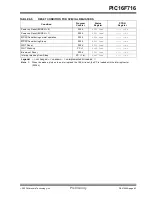


PIC16F716
DS41206A-page 68
Preliminary
2003 Microchip Technology Inc.
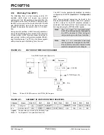
9.12
Watchdog Timer (WDT)
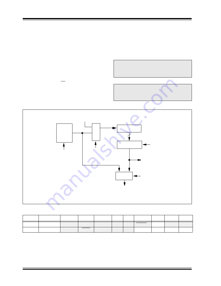
The Watchdog Timer is a free running, on-chip, RC
oscillator which does not require any external
components. This RC oscillator is separate from the
RC oscillator of the OSC1/CLKIN pin. That means that
the WDT will run, even if the clock on the OSC1/CLKIN
and OSC2/CLKOUT pins of the device have been
stopped, for example, by execution of a
SLEEP
instruc-
tion.
During normal operation, a WDT time-out generates a
device Reset (Watchdog Timer Reset). If the device is
in Sleep mode, a WDT time-out causes the device to
wake-up and continue with normal operation (Watch-
dog Timer Wake-up). The TO bit in the Status register
will be cleared upon a Watchdog Timer time-out.
The WDT can be permanently disabled by clearing
configuration bit WDTE (Section 9.1 “Configuration
Bits”).
WDT time-out period values may be found in the
Electrical Specifications section under T
WDT
(parame-
ter #31). Values for the WDT prescaler (actually a
postscaler, but shared with the Timer0 prescaler) may
be assigned using the OPTION_REG register.
.
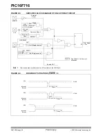
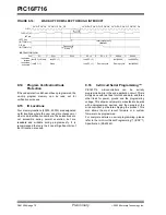
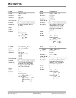
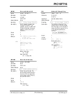
FIGURE 9-14:
WATCHDOG TIMER BLOCK DIAGRAM
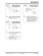
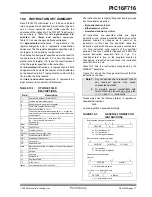
FIGURE 9-15:
SUMMARY OF WATCHDOG TIMER REGISTERS
Note:
The
CLRWDT
and
SLEEP
instructions clear
the WDT and the postscaler, if assigned to
the WDT, and prevent it from timing out
and generating a device Reset condition.
Note:
When a
CLRWDT
instruction is executed
and the prescaler is assigned to the WDT,
the prescaler count will be cleared, but the
prescaler assignment is not changed.
Address
Name
Bits 13:8
Bit 7
Bit 6
Bit 5
Bit 4
Bit 3
Bit 2
Bit 1
Bit 0
2007h
Config. bits
(1)
BORV
(1)
BOREN
(1)
—
—
PWRTE
(1)
WDTE
FOSC1
FOSC0
81h
OPTION_REG
N/A
RBPU
INTEDG
T0CS
T0SE
PSA
PS2
PS1
PS0
Legend:
Shaded cells are not used by the Watchdog Timer.
Note
1:
See Register 9-1 for operation of these bits.
From TMR0 Clock Source (Figure 4-2)
To TMR0 (Figure 4-2)
Postscaler
WDT Timer
WDT
Enable Bit
0
1
M
U
X
PSA
8 - to - 1 MUX
PS2:PS0
0
1
MUX
PSA
WDT
Time-out
8
Note:
PSA and PS2:PS0 are bits in the OPTION_REG register.
Содержание PIC16F716
Страница 6: ...PIC16F716 DS41206A page 4 Preliminary 2003 Microchip Technology Inc NOTES...
Страница 35: ......
Страница 56: ......
Страница 60: ......
Страница 88: ......
Страница 92: ...PIC16F716 DS41206A page 90 Preliminary 2003 Microchip Technology Inc NOTES...
Страница 108: ...PIC16F716 DS41206A page 106 Preliminary 2003 Microchip Technology Inc NOTES...
Страница 110: ...PIC16F716 DS41206A page 108 Preliminary 2003 Microchip Technology Inc NOTES...
Страница 124: ...PIC16F716 DS41206A page 122 Preliminary 2003 Microchip Technology Inc NOTES...


