


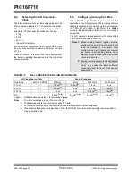

PIC16F716
DS41206A-page 38
Preliminary
2003 Microchip Technology Inc.
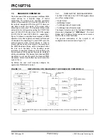
7.4
ENHANCED PWM MODE
The Enhanced PWM mode provides additional PWM
output options for a broader range of control
applications. The module is an upwardly compatible
version of the standard CCP module and offers up to
four outputs, designated P1A through P1D. Users are
also able to select the polarity of the signal (either
active-high or active-low). The module’s Output mode
and polarity are configured by setting the P1M1:P1M0
and CCP1M3:CCP1M0 bits of the CCP1CON register
(CCP1CON<7:6> and CCP1CON<3:0>, respectively).
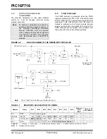
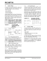
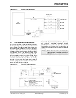
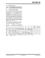
Figure 7-5 shows a simplified block diagram of PWM
operation. All control registers are double buffered and
are loaded at the beginning of a new PWM cycle (the
period boundary when Timer2 resets) in order to
prevent glitches on any of the outputs. The exception is
the PWM Dead-band Delay, which is loaded at either
the duty cycle boundary or the boundary period
(whichever comes first). Because of the buffering, the
module waits until the assigned timer resets, instead of
starting immediately. This means that enhanced PWM
waveforms do not exactly match the standard PWM
waveforms, but are instead offset by one full instruction
cycle (4 T
OSC
).
As before, the user must manually configure the
appropriate TRISB bits for output.
7.4.1
PWM OUTPUT CONFIGURATIONS
The P1M1:P1M0 bits in the CCP1CON register allows
one of four configurations:
• Single Output
• Half-Bridge Output
• Full-Bridge Output Forward mode
• Full-Bridge Output Reverse mode
The Single Output mode is the Standard PWM mode
discussed in Section 7.3 “PWM Mode”. The Half-
Bridge and Full-Bridge Output modes are covered in
detail in the sections that follow.
The general relationship of the outputs in all
configurations is summarized in Figure 7-6.
FIGURE 7-5:
SIMPLIFIED BLOCK DIAGRAM OF THE ENHANCED PWM MODULE
CCPR1L
CCPR1H (Slave)
Comparator
TMR2
Comparator
PR2
(Note 1)
R
Q
S
Duty Cycle Registers
CCP1CON<5:4>
Clear Timer,
set CCP1 pin and
latch D.C.
Note
1:
The 8-bit timer TMR2 register is concatenated with the 2-bit internal Q clock, or 2 bits of the prescaler to create the 10-bit
time base.
TRISB<3>
RB3/CCP1/P1A
TRISB<5>
RB5/P1B
TRISB<6>
RB6/P1C
TRISB<7>
RB7/P1D
Output
Controller
P1M<1:0>
2
CCP1M<3:0>
4
CCP1/P1A
P1B
P1C
P1D
PWM1CON
Содержание PIC16F716
Страница 6: ...PIC16F716 DS41206A page 4 Preliminary 2003 Microchip Technology Inc NOTES...
Страница 35: ......
Страница 56: ......
Страница 60: ......
Страница 88: ......
Страница 92: ...PIC16F716 DS41206A page 90 Preliminary 2003 Microchip Technology Inc NOTES...
Страница 108: ...PIC16F716 DS41206A page 106 Preliminary 2003 Microchip Technology Inc NOTES...
Страница 110: ...PIC16F716 DS41206A page 108 Preliminary 2003 Microchip Technology Inc NOTES...
Страница 124: ...PIC16F716 DS41206A page 122 Preliminary 2003 Microchip Technology Inc NOTES...


