


4-19
15. Measure and note the voltage between TP14 and TP16 (typ. <1mV). Set
the display at 1 and press
Enter
. Measure the voltage once more and
adjust P5 until the difference between the voltages is 120mV
±
200
)
V.
16. Repeat the previous instruction, only this time with the Sensitivity
switch set to position 5. Check that the voltage between TP14 and TP16
is 15mV
±
40
)
V. If necessary, adjust P5 and repeat operation 15.
17. Set the display at 2 and press
Enter
. Measure the resistance between
TP7 and TP10 with the multimeter. Adjust P1 until the voltage is half
the reference voltage between TP10 and TP9 (nom. -0.62v)
±
lmV.
18. Measure the voltage between TP6 and TP10 with the multimeter. Adjust
P2 until the voltage is half the reference current between TP10 and TP9
(nom. 0.62v) +lmV.
19. Measure and note the voltage between LL(+) and RA(-) (typ. <
100
)
V). Set the display at 3 and press
Enter
. Measure the voltage once
more and adjust P4 until the difference between the voltages is 2mV
±
20
)
V. Measure the voltages between the outputs and check that they
are within the limits in the following table:
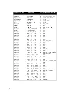
Connectors
Low limit
Nom. Value
High limit
RL - RA
1.20 mV
1.35 mV
1.50 mV
RL-LA 2.40mV
2.65mV 2.90mV
RL-LL
3.00 mV
3.35 mV
3.70 mV
RL-V1
2.70 mV
3.02 mV
3.30 mV
RL-V2
3.30 mV
3.72 mV
4.10 mV
RL-V3
4.00 mV
4.49 mV
5.00 mV
RL-V4
4.50 mV
5.06 mV
5.60 mV
RL-V5
4.00 mV
4.49 mV
5.00 mV
RL-V6
3.30 mV
3.72 mV
4.10 mV
20. Set the display at 4. Set the Base-ohms switch to 500 and the Lead
switch to II. Measure the resistance between LL and RA. Move between
test functions 4 and 5 on the display (remember to press
Enter
), and ad-
just P3 until the difference is 3 ohms
±
0.03 ohms.
Содержание PS-416M
Страница 1: ...1 1 PS 416M User Service Manual PATIENT SIMULATOR...
Страница 4: ...1 4 This page intentionally left blank...
Страница 6: ...1 6 This page intentionally left blank...
Страница 10: ...1 10 This page intentionally left blank...
Страница 12: ...2 12 This page intentionally left blank...
Страница 20: ...4 20 This page intentionally left blank...
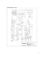
Страница 27: ...5 27 APPENDIX A DIAGRAMS Component Location Diagram Schematic Diagram Part 1 Schematic Diagram Part 2...
Страница 28: ...5 28 This page intentionally left blank...
Страница 29: ...5 29 Component Location...
Страница 30: ...5 30 Schematic Diagram Part 1...
Страница 31: ...5 31 Schematic Diagram Part 2...
Страница 32: ...5 32 This page intentionally left blank...
Страница 34: ...5 34 This page intentionally left blank...
Страница 36: ...5 36...


